 个人中心
个人中心IF输入:2通道
ADC :14 bits
Sample rate:30 MS/s 至 100 MS/s
IF输出:2通道
ADC :14 bits
Sample rate:30 MS/s 至 100 MS/s
ONETEST 欢迎您


IF输入:2通道
ADC :14 bits
Sample rate:30 MS/s 至 100 MS/s
IF输出:2通道
ADC :14 bits
Sample rate:30 MS/s 至 100 MS/s
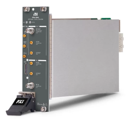
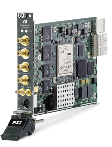
双输入/双输出PXI IF收发仪
PXIe‑5641是一款双输入双输出中频(IF)收发器,适用于射频识别(RFID)测试、频谱监测、实时频谱分析、RF动态测试和软件无线电(SDR)等应用。 该模块可以轻松处理复杂和高速的信号处理、分析和调制任务。
产品编号: 780710-01
Number of channels 2 ADC resolution 14 bits Sample rate 30 MS/s to 100 MS/s Full-scale input range +8.5 dBm peak at 10 MHz ± 1 dB typical (1.7 Vpeak–peak sine, 0.60 VRMS) Maximum input level without damage +24 dBm peak (10Vpeak–peak sine, 3.5 VRMS) Input coupling AC Input impedance 50 Ω nominal Input return loss <-15 dB typical, 250 kHz to 80 MHz Maximum DC input voltage without damage 10 V Average noise density -143 dBm/Hz typical Signal-to-noise ratio >76 dB typical (-1 dBfs at 68 MHz tone, bandwidth = 10 MHz) Maximum instantaneous bandwidth 20 MHz (limited by digital downconverter) Passband flatness (referenced to 10 MHz) 250 kHz to 80 MHz <+0.33 dB, -0.55 dB typical AC coupling cutoff frequency (-3 dB) 50 kHz typical Input group delay variation 10 ns peak-to-peak typical, 250 kHz to 80 MHz Stopband rejection >50 dB typical at 120 MHz, referenced to 10 MHz Third-order intercept (TOI) +38 dBm typicalIF Input
Channel-to-channel crosstalk<40 MHz<-70 dB typical40 MHz to 80 MHz<-60 dB typical IF Input Performance


IF Input Spectral Characteristics
IF Input Spectral Characteristics Performance

Number of channels | Up to 6 per ADC channel |
DDC resolution | 16 bits for both I and Q data |
Decimation[1] | ÷4 to ÷4,096 |
Tuning resolution | ADC clock/232 |


Sample DDC filter performance plots use NI-5640R 1.3 instrument driver library example filter designs. The dark lines in the above figures show the true response of the digital filter in the DDC. The dashed lines show the effect of aliasing after decimation. Notice that for a 10 MHz span, the DDC filter aliasing artifacts have virtually no impact; whereas for a full 20 MHz span, signals at frequency offsets near ±40 MHz can alias back up to -66 dBc within the ±10 MHz passband near the band edges.
Number of channels | 2 |
DAC resolution | 14 bits |
Sample rate | 30 MS/s to 200 MS/s |
Output coupling | AC-coupled |
Output impedance | 50 Ω nominal |
Output return loss | <-15 dB typical, 250 kHz to 80 MHz |
Maximum DC bias voltage without damage | 10 V |
Average noise density | -153 dBm/Hz typical |
| Signal-to-noise ratio+2 dBm output level>69 dB typical-4 dBm output level>64 dB typical | |
| Full-scale output range[2]CIC and inverse sync ON-4 dBm peak at 10 MHz ± 1 dB typical (0.4 Vpeak-peaksine, 0.14 VRMS)Filters off, uncompensated+2 dBm peak at 10 MHz ± 1 dB typical (0.8 Vpeak-peaksine, 0.28 VRMS) | |
Output protection | Indefinite duration short to ground |
Maximum reverse power without damage | +24 dBm peak (10 Vpeak-peak, 3.5 VRMS) |
Passband flatness (referenced at 10 MHz) | <±1 dB typical, 250 kHz to 80 MHz (with CIC and sync compensation filter engaged) |
AC coupling cutoff frequency (-3 dB) | 50 kHz typical |
| Channel-to-channel crosstalk<40 MHz<-70 dB typical≥40 MHz to 80 MHz<-60 dB typical | |


Number of channels | 1 per DAC channel |
DUC resolution | 14 bits for both I and Q data |
Interpolation | 4x to 252x |
Modulation bandwidth | Up to 40 MHz |
Tuning resolution | DAC clock/232. (For example, a 200 MHz clock results in a 46.6 mHz tuning resolution.) |
Conditions | 8-QAM, symbol rate: 3.125 MHz, PRN 9 sequence, power: -5 dBm, filter alpha 0.22, filter length 128, root-raised cosine |
| Modulation error ratio (MER)[3]10 MHz carrier>57 dB typical40 MHz carrier>54 dB typical70 MHz carrier>46 dB typical | |
(Using NI PXIe-1062Q chassis, NI PXIe-8130 controller, single-threaded, half-duplex transfer; transfer rate is dependent upon controller and chassis hardware, software, and backplane usage.)
NI PXIe-5641R to host | 120 MB/s typical |
Host to NI PXIe-5641R | 52 MB/s typical |
Timebase frequency[4] | 200 MHz ± 35 ppm, maximum |
Minimum Sample Clock divisor | 2 for ADC, 1 for DAC |
Supported divisors | 1, 2, 4, 8, and 16 |
Impedance | 50 Ω nominal, AC-coupled |
| Input amplitude rangeSine wave0.63 Vpeak-peak to 2.8 Vpeak-peak (0 dBm to 13 dBm)Square wave0.25 Vpeak-peak to 2.8 Vpeak-peak | |
Maximum input level without damage | +24 dBm (10 Vpeak-peak, 3.5 VRMS) |
Maximum PLL lock time | 250 ms |
External Reference Clock range[5] | 1 MHz to 100 MHz in 1 MHz increments, ±100 ppm |
External Sample Clock range[6] | 30 MHz to 200 MHz |
Modes | Digital input, software |
| SourcesUsing instrument driverTRIG or softwareUsing LabVIEW FPGATRIG, RTSI <0..7> (mapped to PXIe_TRIG<0..7>), or software | |
| SlopeUsing instrument driverRisingUsing LabVIEW FPGARising or falling | |
Impedance | 10 kΩ nominal, DC-coupled |
Range | 0 V to 3.3 V typical, 5 V tolerant |
VIH | 2.2 V typical |
VIL | 0.95 V typical |
Overvoltage protection | -3.5 V to +8 V continuous |
Maximum trigger frequency | <10 MHz typical, system dependent |
Input rise/fall time | <10 ns/V typical |
Number of digital lines | 7 |
I/O direction | Pin-configurable |
Input voltage range | 0 V to 3.3 V typical, 5 V tolerant |
VIH | 2.5 V typical |
VIL | 1 V typical |
VOH | 3.5 V typical, no load |
VOL | 0.1 V typical, no load |
Overvoltage protection | -0.5 to +5.5 V |
Output type | 3.3 V CMOS |
Output current | ±24 mA |
Output impedance | 56 Ω |
+5 V power output voltage | 5 V ± 10% |
+5 V power output current | 500 mA, ±150 mA typical, electronically fused |
Model | Xilinx Virtex 5 SX95T |
Logic cells | 94,208 |
Multipliers/DSP blocks (18 * 18) | 640 |
Block RAM | 8,784 (kbits max) |
Memory size | 128 MB |
Theoretical maximum data rate | 1,600 MB/s |
+3.3 VDC | 3 A |
+12 VDC | 3 A |
Total power | 38.25 W |
Dimensions | 3U, one slot, PXI Express module 21.6 cm * 2.0 cm * 13.0 cm (8.5 in * 0.8 in * 5.1 in) |
Weight | 397 g (13.4 oz) |
| Connector Name | Type | Function |
|---|---|---|
| AI CH <0..1> | SMA | Analog input terminals for the NI PXIe-5641R |
| AO CH <0..1> | SMA | Analog output terminals for the NI PXIe-5641R |
| CLK IN | SMB | Input terminal for an external Reference Clock or Sample Clock |
| TRIG | SMB | Input or output terminal for device trigger signals |
| DIO (AUX I/O) | 9-pin DIN mini-circular | Input or output terminal for device digital I/O (DIO) channels |
Maximum altitude | 2,000 m (800 mbar) (at 25 °C ambient temperature) |
Pollution Degree | 2 |
Indoor use only.
Ambient temperature range | 0 °C to 55 °C |
Relative humidity range | 10% to 90%, noncondensing |
Ambient temperature range | -40 °C to 71 °C |
Relative humidity range | 5% to 95%, noncondensing |
Operating shock | 30 g peak, half-sine, 11 ms pulse |
| Random vibrationOperating5 Hz to 500 Hz, 0.3 grmsNonoperating5 Hz to 500 Hz, 2.4 grms | |
0条提问
X
提问
X
回答
发表口碑
© 2026 Onetest仪器资源库 All Rights Reserved 粤ICP备17028186号-2
 粤公网安备44030902003758