IF频率范围:5GHz至12GHz
带宽:1GHz
调谐分辨率:4.45 μHz
频谱纯度:-97dBc/Hz@7.1 GHz至12 GHz
ONETEST 欢迎您


IF频率范围:5GHz至12GHz
带宽:1GHz
调谐分辨率:4.45 μHz
频谱纯度:-97dBc/Hz@7.1 GHz至12 GHz
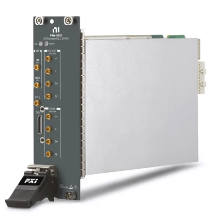
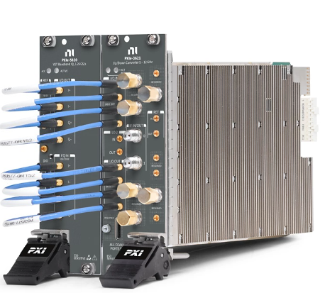
12 GHz,1 GHz带宽PXI矢量信号收发仪
PXIe-5830可支持毫米波频段的验证和生产测试。矢量信号收发仪结合了一个矢量信号发生器、矢量信号分析仪、高速串行接口以及基于FPGA的实时信号处理和控制。PXIe-5830可帮助您测试各种蜂窝和无线标准,如Wi-Fi 6。该仪器采用PXI Express架构,便于扩展测试系统,以支持具有相位相干同步的多输入多输出(MIMO)配置。
产品编号: 787047-01
IF IN/OUT 0, IF IN/OUT 1 frequency range[1] 5 GHz to 12 GHz Frequency bandwidth 1 GHz within the specified frequency ranges Tuning resolution[2] 4.45 μHz The LO2 frequency settling time includes the frequency lock time. Conditions: 20 kHz offset; self-calibration °C ± 5 °C ; LO2 LO Source: Onboard.Frequency
Frequency Range Step Size, Onboard 5 GHz to 12 GHz 2 MHz Frequency Settling Time
Settling Accuracy (Relative to Final Frequency) Settling Time (ms), Onboard 1.0 × 10⁻⁶ 0.50 0.1 × 10⁻⁶ 0.80 0.01 × 10⁻⁶ 1.00 Internal Frequency Reference
LO2 source (Onboard)Initial adjustment accuracy±5 × 10⁻⁶Temperature stability±1 × 10 -6, maximumAging±1 × 10⁻⁶ per year, maximumAccuracyInitial adjustment accuracy ± Aging ± Temperature stability Spectral Purity
Frequency Phase Noise (dBc/Hz, Single Sideband) 5 GHz to 7.1 GHz -103 >7.1 GHz to 12 GHz -97 
| Upconverter Center Frequency | IF IN/OUT 0 (dBm) | IF IN/OUT 1 (dBm) | ||
|---|---|---|---|---|
| Specification | Nominal | Specification | Nominal | |
| 5 GHz to 8 GHz | 14 | 19 | 13 | 18 |
| >8 GHz to 12 GHz | 13 | 17 | 12 | 16 |
The power range refers to continuous wave (CW) average power. For modulated signal generation, it is important to consider the impact of peak to average power ratio (PAPR). For example, a modulated 80 MHz 802.11ax signal with a 11 dB PAPR can be generated with up to +4 dBm average modulated power when the CW average power is 15 dBm. | ||||
Output attenuator resolution | 1 dB, nominal |
Digital attenuation resolution[5] | <0.1 dB |

<0.5 dB of final value | 27 µs, nominal |
<0.1 dB of final value | 40 µs, nominal |
| Upconverter Center Frequency | 23 °C ± 5 °C | 0 °C to 45 °C | ||
|---|---|---|---|---|
| Specification | Typical-95 | Typical | Specification | |
| 5 GHz to 8 GHz | ±1.2 | ±0.8 | ±0.5 | ±1.9 |
| >8 GHz to 12 GHz | ±1.4 | ±1.0 | ±0.6 | ±2.1 |
Conditions: Peak power level -30 dBm to +12 dBm; measured with a CW at 10 MHz offset from the configured upconverter center frequency; measurement performed after the PXIe-5830 has settled; Upconverter/Downconverter Frequency Offset Mode: User-Defined. This specification is valid only when the module is operating within the specified ambient temperature range and within ±5 °C from the last self-calibration temperature, as measured with the onboard temperature sensors. This specification requires that temperature correction is being performed. Temperature correction is applied automatically if NIRFSG_ATTR_AUTOMATIC_THERMAL_CORRECTION is enabled (default). Temperature correction is applied if necessary only when NI-RFSG settings are adjusted. If NIRFSG_ATTR_AUTOMATIC_THERMAL_CORRECTION is disabled, the niRFSG_PerformThermalCorrection must be explicitly called. | ||||
| Upconverter Center Frequency | Relative Amplitude Accuracy (dB) |
|---|---|
| 5 GHz to 8 GHz | ±0.25 |
| >8 GHz to 12 GHz | ±0.30 |
Conditions: Peak power level -30 dBm to +12 dBm; measured with a CW at 10 MHz offset from the configured upconverter center frequency; measurement performed after the PXIe-5830 has settled; Upconverter/Downconverter Frequency Offset Mode: User-Defined. Relative accuracy describes the residual absolute accuracy error when compared to the absolute accuracy error at 0 dBm. This specification is valid only when the module is operating within the specified ambient temperature range and within ±5 °C from the last self-calibration temperature, as measured with the onboard temperature sensors. This specification requires that temperature correction is being performed. Temperature correction is applied automatically if NIRFSG_ATTR_AUTOMATIC_THERMAL_CORRECTION is enabled (default). Temperature correction is applied if necessary only when NI-RFSG settings are adjusted. If NIRFSG_ATTR_AUTOMATIC_THERMAL_CORRECTION is disabled, the niRFSG_PerformThermalCorrection must be explicitly called. | |
| Upconverter Center Frequency | 23 °C ± 5 °C | 0 °C to 45 °C | ||
|---|---|---|---|---|
| Specification | Typical-95 | Typical | Specification | |
| 5 GHz to 8 GHz | 1.8 | 1.2 | 1.1 | 2.2 |
| >8 GHz to 12 GHz | 1.9 | 1.3 | 1.1 | 2.2 |
Conditions: Peak power level -30 dBm to +10 dBm; module temperature within ±5 °C of last self-calibration temperature. Frequency response is defined as the maximum relative amplitude deviation from the reference offset frequency. For the PXIe-5830 IF output, the reference offset frequency is 10 MHz higher than the upconverter center frequency. For the absolute amplitude accuracy at the reference offset, refer to the IF Output Amplitude Accuracy section. | ||||


| Upconverter Center Frequency | Output Power Level Setting | ||
|---|---|---|---|
| -10 dBm | 0 dBm | 15 dBm | |
| 5 GHz to 8 GHz | -156 | -149 | -135 |
| >8 GHz to 12 GHz | -154 | -148 | -135 |
Conditions: 10 averages; 40 dB baseband signal attenuation; noise measurement frequency offset by 200 MHz from the upconverter center frequency; the instrument driver is in peak mode. Measured on the PXIe-3621 IF IN/OUT 1 port. The IF IN/OUT 0 port has a 1 dB to 5 dB degradation compared to the IF IN/OUT 1 port. | |||
| Upconverter Center Frequency | IF IN/OUT 0 | IF IN/OUT 1 | ||||
|---|---|---|---|---|---|---|
| Output Power Level Setting | Output Power Level Setting | |||||
| -30 dBm | 0 dBm | 15 dBm | -30 dBm | 0 dBm | 15 dBm | |
| 5 GHz to 8 GHz | -56 | -56 | -49 | -45 | -46 | -46 |
| >8 GHz to 12 GHz | -58 | -57 | -41 | -53 | -52 | -39 |
Conditions: Measured by generating two -7 dBFS tones centered at +100 MHz within the instantaneous bandwidth with 10 MHz separation. | ||||||
| Frequency | Offset ≤ 500 kHz | 500 kHz < Offset ≤ 20 MHz | Offset > 20 MHz[6] |
|---|---|---|---|
| 5 GHz to 8 GHz | -62 | -44 | <-70 |
| >8 GHz to 12 GHz | -59 | -51 | <-70 |
Conditions: Output full scale level 0 dBm. Measured with a single tone at 0 dBFS. NoteOffset refers to ± desired signal offset (Hz) around the current LO frequency. | |||
| Frequency | 0 Hz ≤ Offset ≤ 5 MHz |
|---|---|
| 5 GHz to 7.1 GHz | -64 |
| >7.1 GHz to 12 GHz | -46 |
Conditions: Output full scale level 0 dBm. NoteOffset refers to ± desired signal offset (Hz) around the current LO frequency. | |
| Upconverter Center Frequency | Self-Calibration °C ± 1 °C | Self-Calibration °C ± 5 °C |
|---|---|---|
| 5 GHz to 8 GHz | -50 | -47 |
| >8 GHz to 12 GHz | -48 | -36 |
Conditions: Peak output power -30 dBm to +15 dBm. Input tone power at a maximum of -3 dBr. LO2 LO Source property set to Onboard. LO Residual Power averaged across a maximum of 1 GHz bandwidth. | ||

| Upconverter Center Frequency | Self-Calibration °C ± 1 °C | Self-Calibration °C ± 5 °C |
|---|---|---|
| 5 GHz to 8 GHz | -39 | -34 |
| >8 GHz to 12 GHz | -48 | -41 |
Conditions: Peak output power levels -30 dBm to +15 dBm. Input tone power at a maximum of -3 dBr. LO2 LO Source property set to Onboard. This specification describes the maximum residual sideband image within the 1 GHz device instantaneous bandwidth. | ||


Amplitude range | Average noise level to +20 dBm (CW RMS) |
Gain resolution | 1 dB, nominal |
| Downconverter Center Frequency | IF Analog Gain Range (dB) |
|---|---|
| 5 GHz to 8 GHz | ≥61 |
| >8 GHz to 12 GHz | ≥57 |
<0.5 dB of final value | 27 µs, nominal |
<0.1 dB of final value | 40 µs, nominal |
| Downconverter Center Frequency | 23 °C ± 5 °C | 0 °C to 45 °C | ||
|---|---|---|---|---|
| Specification | Typical-95 | Typical | Specification | |
| 5 GHz to 8 GHz | ±1.2 | ±0.8 | ±0.5 | ±1.6 |
| >8 GHz to 12 GHz | ±1.4 | ±1.0 | ±0.7 | ±1.6 |
Conditions: Reference level -30 dBm to +30 dBm; measured with a CW at 10 MHz offset from the configured downconverter center frequency when a user-defined frequency offset is not applied; measurement performed after the PXIe-5830 has settled; Upconverter/Downconverter Frequency Offset Mode: User-Defined. This specification is valid only when the module is operating within the specified ambient temperature range and within ±5 °C from the last self-calibration temperature, as measured with the onboard temperature sensors. | ||||
| Downconverter Center Frequency | Relative Amplitude Accuracy (dB) |
|---|---|
| 5 GHz to 8 GHz | ±0.25 |
| >8 GHz to 12 GHz | ±0.40 |
Conditions: Reference level -30 dBm to +30 dBm; measured with a CW at 10 MHz offset from the configured downconverter center frequency; measurement performed after the PXIe-5830 has settled; Upconverter/Downconverter Frequency Offset Mode: User-Defined. Relative accuracy describes the residual absolute accuracy error when compared to the absolute accuracy error at 0 dBm. This specification is valid only when the module is operating within the specified ambient temperature range and within ±5 °C from the last self-calibration temperature, as measured with the onboard temperature sensors. | |
| Downconverter Center Frequency | 23 °C ± 5 °C | 0 °C to 45 °C | ||
|---|---|---|---|---|
| Specification | Typical-95 | Typical | Specification | |
| 5 GHz to 8 GHz | 2.2 | 1.8 | 1.2 | 2.8 |
| >8 GHz to 12 GHz | 2.3 | 2.0 | 1.1 | 3.2 |
Conditions: Input reference level -30 dBm to +20 dBm; module temperature within ±5 °C of last self-calibration temperature. Frequency response is defined as the maximum relative amplitude deviation from the reference offset frequency. For the PXIe-5830 IF input, the reference offset frequency is 10 MHz higher than the downconverter center frequency. For the absolute amplitude accuracy at the reference offset, refer to the IF Input Amplitude Accuracy section. | ||||


| Downconverter Center Frequency | -30 dBm Reference Level | 0 dBm Reference Level |
|---|---|---|
| 5 GHz to 8 GHz | -162 | -142 |
| >8 GHz to 12 GHz | -162 | -142 |
Conditions: Input terminated with a 50 Ω load; 10 averages; noise measurement frequency offset 6 MHz to output frequency. Measured on the PXIe-3621 IF IN/OUT 1 port. The IF IN/OUT 0 port has a 2 dB degradation compared to the IF IN/OUT 1 port. | ||
| Downconverter Center Frequency | Reference Level | ||
|---|---|---|---|
| -30 dBm | 0 dBm | 15 dBm | |
| 5 GHz to 8 GHz | -6 | 20 | 35 |
| >8 GHz to 12 GHz | -4 | 19 | 33 |
Conditions: Measured by generating two -6 dBFS tones centered at +100 MHz within the instantaneous bandwidth with 10 MHz separation. | |||
| Frequency | 60 kHz ≤ Offset ≤ 60 kHz | Offset ≥ 60 MHz[7] |
|---|---|---|
| 5 GHz to 8 GHz | -74 | -74 |
| >8 GHz to 12 GHz | -75 | -75 |
Conditions : Reference level 0 dBm. Measured with the IF IN 1 port terminated with 50 Ω. NoteOffset refers to ± desired signal offset (Hz) around the current LO frequency. | ||
| Downconverter Center Frequency | Self-Calibration °C ± 1 °C | Self-Calibration °C ± 5 °C |
|---|---|---|
| 5 GHz to 8 GHz | -54 | -44 |
| >8 GHz to 12 GHz | -47 | -38 |
Conditions: Reference level is -30 dBm to +15 dBm. Input tone power at a maximum of -3 dBr. LO2 LO Source property set to Onboard. LO Residual Power averaged across a maximum of 1 GHz bandwidth. | ||

| Downconverter Center Frequency | Self-Calibration °C ± 1 °C | Self-Calibration °C ± 5 °C |
|---|---|---|
| 5 GHz to 8 GHz | -47 | -39 |
| >8 GHz to 12 GHz | -51 | -42 |
Conditions: Peak output power levels -30 dBm to +15 dBm. LO2 LO Source property set to Onboard. This specification describes the maximum residual sideband image within the 1 GHz device instantaneous bandwidth. | ||


The following measurements were taken using RFmx and corresponding RFmx default values.
| I/Q Carrier Frequency | Signal Bandwidth | |
|---|---|---|
| 80 MHz | 160 MHz | |
| 5.1 GHz to 7.2 GHz | -50 | -47 |


| I/Q Carrier Frequency | NR Carrier Configuration | ||
|---|---|---|---|
| 1 x 100 MHz[15] | 2 x 100 MHz[16] | 1 x 400 MHz[17] | |
| 5 GHz to 8 GHz | -50 | -47 | -43 |
| >8 GHz to 12 GHz | -49 | -46 | -43 |
Conditions: IF average power level is -25 dBm to 0 dBm. LO2 LO Source: SG_SA_Shared. | |||
| I/Q Carrier Frequency | 1 x 100 MHz[15] | 2 x 100 MHz[16] | 1 x 400 MHz[17] |
|---|---|---|---|
| 5 GHz to 8 GHz | -41 | -41 | -40 |
| >8 GHz to 12 GHz | -39 | -39 | -38 |
Conditions: IF average power level is -25 dBm to 0 dBm. LO2 LO Source: Onboard. | |||


Refer to the PXIe-5820 Specifications for more information about characteristics of the PXIe-5820 front panel input and output.
| I/Q INConnectorsMMPX (female)Input coupling, per terminalDCInput typeDifferentialDifferential impedance100 Ω | |
| I/Q OUTConnectorsMMPX (female)Output coupling, per terminalDCOutput typeDifferentialNumber of channels2Impedance100 Ω | |
| LO2 INConnectorsMMPX (female)Frequency range3.55 GHz to 7.1 GHzInput power range[21]+6 dBm to +10 dBm, nominalInput return loss10 dB, nominalAbsolute maximum input power+10 dBmLO2 couplingDC coupled to groundImpedance50 Ω | |
| LO2 OUTConnectorsMMPX (female)Frequency range3.55 GHz to 7.1 GHzAbsolute maximum output power+10 dBmLO2 CouplingDC coupled to groundOutput power resolution[22]0.5 dB, nominalImpedance50 ΩOutput return loss10 dB, nominal | |
| DIOConnectorMini HDMI | |
| IF IN/OUTConnectorsSMA 27 GHz (female)Impedance50 Ω during active mode, ∞ impedance after reboot and resetCouplingAC coupled to groundAbsolute maximum input power+25 dBm |


| REF IN/OUTConnectorsMMPX (female)Frequency10 MHzInput tolerance[23]±10 × 10-6Input amplitude[24]0.7 V pk-pk to 3.3 V pk-pk , typicalCouplingDCOutput amplitude1.65 V pk-pk into 50 Ω, nominalImpedance50 Ω |
| Module | +3.3 VDC | +12 VDC | Total Power (W) |
|---|---|---|---|
| PXIe-5820 | 3.3 A (10.89 W) | 6.0 A (72.0 W) | 82.89 |
| PXIe-3621 | 5.0 A (6.93 W) | 5.0 A (67.2 W) | 74.13 |
| PXIe-5830 (combined instrument) | — | — | 157.02 |
Interval | 1 year |
| Module | Dimensions | Weight | |
|---|---|---|---|
| Grams | Ounces | ||
| PXIe-5820 | 3U, 2 slots | 795 | 28.0 |
| PXIe-3621 | 3U, 2 slots | 1,066 | 37.6 |
| PXIe-5830 (combined instrument) | 3U 4 slots | 1,861 | 65.6 |
| TemperatureOperating0 °C to 45 °CStorage-41 °C to 71 °C | |
| HumidityOperating10% to 90%, noncondensingStorage5% to 95%, noncondensing | |
Pollution Degree | 2 |
Maximum altitude | 2,000 m (800 mbar) (at 25 °C ambient temperature) |
| Shock and VibrationOperating vibration5 Hz to 500 Hz, 0.3 g RMSNon-operating vibration5 Hz to 500 Hz, 2.4 g RMSOperating shock30 g, half-sine, 11 ms pulse | |
0条提问
X
提问
X
回答
发表口碑
© 2026 Onetest仪器资源库 All Rights Reserved 粤ICP备17028186号-2
 粤公网安备44030902003758