是德科技 | KEYSIGHT
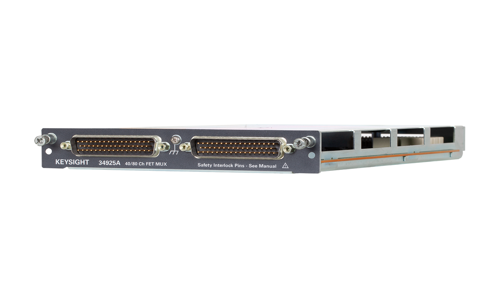
34925A 开关系统 40/80通道 详细指标
Modular Module BERTs, Digitizers, and DAQs
Offset voltage 3 < 3 μV < 3 μV <
50 μV
< 100 uV 1-wire < 50 uV <
3 μV
DC Isolation (ch-ch, ch-earth) > 10 GΩ > 10 GΩ > 10 GΩ > 10 GΩ >
10 GΩ
Leakage current 3 N/A N/A N/A N/A 20 nA
9
T/C cold junction accuracy 3, 10 <
1°C N/A N/A N/A N/A
Bandwidth at terminal block 4 45 MHz 25 MHz 45 MHz
5/4 MHz
10 MHz 1-wire 25 MHz 5/4 MHz 11
1 MHz
Crosstalk at terminal block (ch-ch)
4
300 kHz - 75 dB - 75 dB - 75 dB - 75 dB Not recommended for
RF signal switching 1 MHz 20 MHz
45 MHz
- 75 dB
- 50 dB
- 40 dB
- 75 dB
- 50 dB
- 75 dB
- 50 dB
- 40 dB
- 70 dB
- 45 dB
LO – earth 150 pF 150 pF
250 pF
200 pF
130 pF
120 pF
200 pF
170 pF
100 pF
Rated load 100 M 10 M
100 k
100 M
10 M
100 k
1000 M
10 M
10 k
1000 M
10 M
10 k
Scanning speeds 7 100 ch/sec 100 ch/sec 500 ch/sec 500 ch/sec
1000 ch/sec
Open/ close time, typical 4 ms/4 ms 4 ms/4 ms 0.5 ms/0.5 ms 0.5 ms/0.5 ms
0.25 ms/0.25 ms
Analog bus backplane Yes Yes Yes Yes Yes
条件:4. 50 Ω source, 50 Ω load, differential measurements verified with 4 -port network analyzer (Sdd21)
5. With input resistors bypassed. Bypassing resistors will reduce the lifetime of relays. See the rated load relay life
9. Ambient temperature < 30°C
10. Includes 0.5°C temperature reference sensor and 0.5°C terminal block isothermal gradient error, measured under
11. With input protection resistors: 2 x 100 Ω ±5%; 0.5W; TC = ±200 ppm/°C. The series resistance of the 34923/24/25
12. Channel resistance is typically < 1.5 Ω but can go as high as 50 Ω when a channel is used in measurement
than 1 week. Switching relays for 2K cycles prior to use may reduce the variation in channel resistance. Applies to
The 34980A matrix modules are full Crosspoint matrices that allow you to connect any row to any column.
This is a convenient way to connect multiple test instruments to multiple points on a device under test.
Notes: 1. DC or AC RMS voltage, channel -to -channel or channel -to -earth 2. Peak voltage, channel -to -channel or channel -to -earth 3. Into analog bus. System errors are included in the internal DMM measurement accuracy specifications
characteristics. 6. Limited to 6 W of channel resistance power loss per module 7. Speeds are for 2 -wire ohms or DCV, 4 1/2 digits, delay 0, display off, autozero off, and within the bank
8. DC or peak AC current
worst -case loading of the mainframe; see User’s Guide for information on supported external reference sensors
limits the use of the
100 Ω range.
applications with <
10 mA load current. Increased relay channel resistance for measurements with load currents
below
10 mA can occur on cards that have been out of service or following relay inactivity for periods of greater
the 34921A and 34922A. Keysight recommends the use of 4 -wire Ohms for resistance measurements. For high
accuracy voltage measurements, select the DMM input resistance setting of >10 G ohms to minimize the impact of
relay contact resistance. 13. Pollution Degree 1 ±300Vrms or VDC; Pollution Degree 2 ±100Vrms or VDC 14. Pollution Degree 1 ±150Vpeak; Pollution Degree 2 ±100Vpeak
34980A Matrix Switch Modules
Choose from the following features
• Latching armature relays— Max 300 Vrms or DC
1 A
• High-speed reed relays— Max 150 Vpeak
0.5 A
• Configurable dual 4x8, dual 4x16, or quad
4x32 modules
• Single-wire configuration (34933A or 34934A)
• High-density matrix with automatic surge protection and row disconnects for flexible measurements
(34934A)
• Analog bus expandable rows to create larger matrices
• Connections via standard
50 or 78-pin D-sub cables or detachable terminal block
Each cross-point in the matrix switch has two wires—a high and a low for the measurement. Or, if you
prefer, the
34933A and 34934A can be configured as a single-wire matrix, increasing the number of
Figure 5. 34932A dual
4x16 armature matrix
The 34933A also has in-rush resistors on each column for added protection. The
34934A also has in- rush
protection resistors but also has an automatic bypass switch for flexibility in making low -level
measurements. Row disconnect switches also reduce the capacitance loading when combining modules
to create larger matrices
条件:to create a larger matrix. The matrix can then be connected to the internal DMM for easy measurements.
Multiple matrix modules can be combined through the analog bus or the row expansion kit (34934A only)
Combine your matrix with a multiplexer switch to achieve the desired switching topology and get a lower -
cost solution with better specifications. All the matrix switches include a relay counter to help predict when
relays need to be replaced. Use the sequencing feature to easily change between different cross -point
NOTE: The 34933A and 34934A have
100-ohm input protection resistors to limit current and protect the
Figure 6. 34934A quad
4x32 matrix (1 of 4 matrices shown)
Matrix switch modules 34931A 34932A 34933A
34934A
Channels/configurations dual 4x8 8x8
4x16
8x16
4x32
8x8
4x16
4x128
8x64
16x32
Switch type Armature latching Armature latching Reed non-latching Reed non-latching
Max volts ± 300 V 1, 13 ± 300 V 1, 13 ± 150 Vpeak 2, 14
± 100 Vpeak
条件:Initial closed channel res 3 < 1.5 Ω < 1.5 Ω < 1.5 Ω 5/200 Ω 8 nominal < 1Ω/100 Ω 8, 10
Switch current 1 A 1 A 0.5 A 5/0.05 A
8
0.5 A
Carry current 2 A 2 A 1.5 A 5/0.05 A
0.5 A
Power (VA) 6 60 VA 60 VA 10 VA 7, 8, 9 10 VA 2, 8
10
Volt-Hertz limit 10^8 10^8 10^8
10^8
Offset voltage 3 < 3 uV < 3 uV <
50 uV
< 20 uV
DC Isolation (ch-ch, ch-earth) > 10G Ω 12 > 10G Ω 12 > 10G Ω
10G Ω
Bandwidth at terminal block 4 30 MHz 30 MHz 30 MHz 5/4 MHz
8
Crosstalk at terminal block (ch-ch)
4
300 kHz –65 dB –65 dB –65 dB
–65 dB
1 MHz
20 MHz
–55 dB
–30 dB
–55 dB
–30 dB
–55 dB
–40 dB
–55 dB
–33 dB
LO – earth 50 pF 80 pF
50 pF
80 pF
80 pF
75 pF
45 pF
250 pF
条件:4. 50 Ω source, 50 Ω load, differential measurements verified (Sdd21)
5. With input resistors bypassed. Bypassing resistors will reduce the lifetime of relays. See the rated load relay life
characteristics. 6. Limited to 6 W channel resistance power loss per module 7. Power restrictions allow only 20 channels to be closed at one time 8. Protection Resistors:
9. 34933A - 100Ω ± 5%; 0.5W; TC = ±200ppm/°C.
10. 34934A - 100Ω ± 1%; 0.25W; TC = ±100ppm/°C.
11. If this resistance is not bypassed in the low side source line of 4- wire resistance measurement, the 100 Ω range is
than 1 week. Switching relays for 2K cycles prior to use may reduce the variation in channel resistance. Applies to
The 34980A general-purpose switches can be used to route signals or to control other system devices.
These switches are ideal for device actuation and switching loads or power supplies.
No-load 100 M 100 M
1000 M
1000 M operations 10 V
100 mA
Rated load 10 M 100 k
10 M
100 k
10 M
10 k
Open/close time 4 ms/4 ms 4 ms/4 ms 0.5 ms/0.5 ms
0.35 ms/0.10 ms
Analog bus backplane connection Bank 2 Bank 2 Bank
2 No
Notes: 1. DC or AC RMS voltage, channel -to -channel or channel -to -earth 2. Peak voltage, channel -to -channel or channel -to -earth 3. Into analog bus. System errors are included in the internal DMM measurement accuracy specifications
limited. 12. Channel resistance is typically < 1.5 Ω but can go as high as 50 Ω when a channel is used in measurement applications with < 10 mA load current. Increased relay channel resistance for measurements with load currents below
10 mA can occur on cards that have been out of service or following relay inactivity for periods of greater
the 34931A and 34932A. Keysight recommends the use of 4 -wire Ohms for resistance measurements. For high
accuracy voltage measurements, select the DMM input resistance setting of >
10 G ohms to minimize the impac t of
relay contact resistance. 13. Pollution Degree 1 ±300Vrms or VDC; Pollution Degree 2 ±100Vrms or VDC 14. Pollution Degree 1 ±150Vpeak; Pollution Degree 2 ±100Vpeak
34980A General-Purpose Switch Modules
Choose from the following features
• Form C channels up to 1 A
60 VA
• Form A channels up to 5 A
150 VA
• Simultaneous channel switching
条件:• Temperature sensor to detect overheating conditions
• Connections via standard
50 or 78-pin Dsub cables or detachable terminal block
The 34937A is the most versatile general-purpose switch with 28 Form C channels that can switch up to 1
A of current. In addition, this module has four Form A channels that can switch up to 5 A of current. For
power switching applications, the 34938A has 20
5-amp channels in a Form A topology. Each Form A
general-purpose switch can handle up to 150 W, enough for many power line switching applications. For
high-density applications, the 34939A offers
64 Form A channels for switching up to 1A and carrying
currents up to 2A.
The general purpose switches contain latching armature relays where multiple channels can be closed at
the same time. Additionally, for switching reactive loads, the optional terminal blocks have pads for
条件:The built-in relay counter helps predict when relays need to be replaced.
Figure 7. 34937A
32-channel Form A / Form C
General purpose switch modules 34937A 34938A
34939A
Channels/configurations
28 Form C
4 Form A 20 Form A
64 Form A
Switch Type Armature, latching Armature, latching Armature, latching
最大 volts (DC, AC RMS, 峰值)
Form C – 300 VAC/DC 1, 4
7
Form A – 30 VDC/250 VAC 5 30 VDC/250 VAC 1, 5 +/- 100 V peak
6
Form C – 1 A (2 A carry)
Form A – 5 A switch
(7 A carry)
5 A switch
(7 A carry)
1 A switch
(2 A carry)
Power (VA)2 Form C – 60 VA
Form A – 150 VA 150 VA
60 VA
Volt-Hertz limit 108 108
108
Offset voltage 3 µV 3 µV
3 µV
Initial closed channel resistance
8 Form C – 125 mΩ
Form A – 50 mΩ < 60 mΩ <
125 mΩ
CD isolation (ch-ch, ch-earth) > 10 GΩ > 10 GΩ
10 GΩ
Bandwidth at terminal block 3 10 MHz 1 MHz
10 MHz
Channel isolation at terminal block
3
100 kHz
1 MHz
10 MHz
55 dB
35 dB
15 dB
60 dB
40 dB
45 dB
25 dB
5 dB
Form C 12 pF, Form A
10 pF
Form C 21 pF, Form A
18 pF
65 pF
105 pF
20 pF
70 pF
Relay life no-load/rated Form C – 100 M/100 k
Form A – 50 M/30 k 50 M/30 k >
100 M/100 k
Open/close time Form C – 4 ms/4 ms
Form A – 10 ms/10ms 10 ms/10ms
4 ms/4ms
Analog bus backplane connection No No No
条件:4. Pollution Degree 1 ±300Vrms or VDC; Pollution Degree 2 ±100Vrms or VDC
5. Pollution Degree 1 ±250Vrms or VDC; Pollution Degree 2 ±100Vrms or VDC
6. Peak voltage, channel -to -channel or channel -to -earth
7. Differential Voltage FormC – FormA:
8. Channel resistance is typically < 1.5 Ω but can go as high as 50 Ω when a channel is used in measurement
than 1 week. Switching relays for 2K cycles prior to use may reduce the variation in channel resistance. Applies to
Notes: 1. DC or AC RMS voltage, channel -to -channel or channel -to -earth 2. Limited to 6 W of channel resistance power loss per module 3. 50 Ω source
50 Ω load, differential measurements verified (S21)
Pollution Degree
300Vrms or Vdc
Pollution Degree
100Vrms or VDC
applications with <
10 mA load current. Increased relay channel resistance for measurements with load currents
below
10 mA can occur on cards that have been out of service or following relay inactivity for periods of greater
the 34937A
34938A and 34939A
34980A RF and Microwave Switch Modules
The
34980A offers a variety of RF and microwave switch modules—RF multiplexers, SPDT switching
from DC to 26.5 GHz, or a switch/ attenuator driver module that allows you to control switches or
attenuators external to the
34980A mainframe.
34941A/42A—from DC to 3 GHz
The RF switch modules can be used to switch signals from DC to 3 GHz and above. This can be useful
for switching signals between oscilloscopes, spectrum analyzers, network analyzers, and other RF test
Choose from the following features
条件:The 34941A and 34942A are configured as four independent 1x4 RF multiplexers on a single module.
• 50- or 75-ohm Quad
4-channel multiplexers
• DC to 3 GHz
Multiple banks can be connected together to create a larger multiplexer. To prevent ground loops,
individual multiplexers are isolated from each other and from the mainframe’s chassis. However, the
multiplexer channels can be chassis grounded with a simple change. Both
50- ohm and 75-ohm versions
条件:with the unterminated switches or select the terminated switches to maintain an impedance match.
Figure 8. 34941A Quad 1x4 50 ohm
3 GHz multiplexer
Figure 9.
34941A typical initial crosstalk
Figure 10.
34941A typical initial insertion loss
Figure 11.
34941A typical initial VSWR
Figure 12.
34942A typical initial crosstalk
34946A/47A—From DC to 26.5 GHz
For applications where you need only a few high-frequency switches, the
34946A and 34947A offer ingle-
pole, double-throw switches in either 4GHz
20GHz or 26.5GHz options. These modules internally mount
two or three independent Keysight N1810 series coaxial switches. These switches are well known for
their excellent insertion loss, isolation, and VSWR specifications.
Switch read-back capabilities allow you to query the position of the switch. You can choose higher density
These modules can also be ordered without switches installed. This gives you the capability to install your
own N1810 series switches or use the module to control the N1810 Series switches outside the
Figure 13.
34942A typical initial VSWR
Figure 14.
34942 typical initial insertion loss
N1810 minimum required switch options Option Comment
Coil Voltage option 124
24 VDC coil
DC Connector option 201 D” subminiature
9 pin female
Drive option
402 Position indicators
Figure 15. 34946A Dual
1x2 SPDT terminated microwave switch
DC to 3 GHz DC to 26.5 GHz
3
34941A 34942A 34946A
34947A
Channels quad 1x4 quad 1x4 2 SPDT
3 SPDT
Switch Type
50 Ω unterminated
latching relays 75 Ω unterminated, latching relays 50 Ω terminated
50 Ω unterminated
mainframe · RF characteristics
Frequency range
2 DC to 3 GHz DC to 1.5 GHz DC to 4 GHz
20 GHz or 26.5 GHz
DC to 4 GHz,
20 GHz or 26.5 GHz
Insertion loss 2 <
40C/80% RH)
100 MHz
1 GHz
3 GHz
0.15 dB
0.60 dB
1.40 dB
0.15 dB
0.60 dB
VSWR 100 MHz 1 GHz 1.03 1.25 1.55 1.15 1.35
3 GHz
100 MHz
1 GHz
3 GHz
Contact factory 80 dB 58 dB
40 dB
Contact factory 80 dB
60 dB
Spurious noise below 1.3 GHz -140 dBm -140 dBm 80 dB
80 dB
Rise time < 80 ps <
160 ps N/A N/A
Signal delay < 1 ns <
1 ns N/A N/A
Capacitance < 30 pF <
30 pF N/A N/A
七、Switching Specifications
Max volts 1 30 V 30 V 7 VDC
7 VDC
Max current 0.5 A
0.5 A N/A N/A
Max power 10 W 5 10 W 5 1 W@7 VDC,50 W peak 4 1 W@7 VDC,50 W peak
4
Offset voltage 10 µV
10 µV N/A N/A
Initial channel resistance 6 1 Ω
1 Ω N/A N/A
Volt-Hertz limit 2 x 10¹⁰ 2 x
1010
Relay life 300,000 at 30 V/10 mA load
100,000 at 10 W load RF SAmeas
300,000 at 30 V/10 mA
> 5 M cycles >
5 M cycles
Open/close time 18 ms/18 ms 18 ms/18 ms < 15 ms/15 ms <
15 ms/15 ms
Connector type Female SMA Mini
75 Ω SMB Female SMA Female SMA
Coil voltage N/A N/A 24 VDC
24 VDC
Analog bus backplane connection No No No No
条件:4. 10 usec maximum duration
5. Max power is 1 W between 30 MHz and 1 GHz for CISPR 11 compliance
6. Channel resistance is typically < 1.5 Ω but can go as high as 50 Ω when a channel is used in measurement
than 1 week. Switching relays for 2K cycles prior to use may reduce the variation in channel resistance. Applies to
Note: 1. Channel -to -earth 2. 50 Ω source, 50 Ω load (75 Ω for 34942A)
3. For more detailed switch specifications, see the Keysight N1810TL, N1811TL, N1812UL for 34946A, and N1810UL
applications with <
10 mA load current. Increased relay channel resistance for measurements with load currents
below
10 mA can occur on cards that have been out of service or following relay inactivity for periods of greater
34945A/34945EXT Microwave Switch/Attenuator
条件:standard SPDT switches. The 34945A /EXT can be extended by adding additional 34945EXT boards.
simultaneous switching, you can connect an external power supply to the 34945EXT.
This module allows you to control switches, attenuators, and other devices external to the
34980A. The
34945A / 34945EXT provides the power and control signals for many of the most popular microwave
switches and attenuators. One 34945A /34945EXT combination can drive up to 64 switch coils —that’s
32
The first 34945EXT is powered by the mainframe. You can add up to seven additional
34945EXT boards
with user-supplied power. Multiple switch operations are performed in sequential order, or for faster,
The Y1150A-Y1155A distribution boards enable simple connections to the external switches. The
distribution boards plug onto the 34945EXT and are used to route the power and control signals from the
driver module to the switches using standard cables
The
34945A /34945EXT also has sensing capabilities that allow a read back of the actual position of the
switch or attenuator. Drive signals for LED indicators are also provided to give a visual indication of the
switch position. The following microwave switches and attenuators are supported by the Y1150AY1155A
• N181x/U9397x series SPDT switches
• 8762/3/4 series SPDT switches (screw terminals)
• 8765x coaxial switches
• 8766x/8767x/8768x multiport switches
• 87104x/106x/L710xx/L720xx multiport switches
• 87406x series matrix switches
• 87204x/206x series multiport switches
• 87606x series matrix switches
• 87222x/L7222 transfer switches
• 849x and 8490x series attenuators
• Other switches and devices through individual screw terminal connections
Figure 16.
34945A/34945EXT
34945EXT switch drive (64 channels, low side drive mode)
以上指标摘自厂家官方数据手册,完整定义、测试条件与保证值口径以手册为准。完整指标、测试条件与定义口径请见产品页「软件和手册 | 白皮书」栏目中的官方数据手册。
是德科技 | KEYSIGHT · onetest 仪器资源库



 客服








 粤公网安备44030902003758