是德科技 | KEYSIGHT
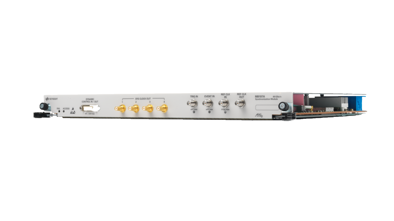
M8197A 240MHz 模块 详细指标
Modular AXI Waveform and Function Generators
Sample rate
53.76 GSa/s to 65.00 GSa/s
or 26.88 GSa/s to 32.50 GSa/s (sample rate divider =
2)
or 13.44 GSa/s to 16.25 GSa/s (sample rate divider =
4)
Number of channels per M8195A module 1, 2 or 4 (corresponds to option 001, 002
004)
In “Single channel duplicate mode” the signal on channel 1 is duplicated on channel 3, channel
2 and
channel 4 are unused. In “Dual channel duplicate mode” the signal on channel
1 is duplicated on channel
3 and the signal on channel 2 is duplicated on channel
4.
This mode allows differential signals to be generated with adjustable skew between normal and
Int. Memory A waveform segment is continuously repeated
Ext. Memory A waveform segment/sequence/scenario is continuously repeated
Int. Memory A waveform segment is looped continuously after a trigger event is received
Ext. Memory A waveform segment/sequence/scenario is generated once after a trigger event is received
Int. Memory A waveform segment is looped continuously after a rising edge of the trigger/gate input
Ext. Memory A waveform segment/sequence/scenario is generated if the trigger/gate input is high
Internal sample memory
1 MSa per module
(for modes of operation see Sample memory modes table below)
Extended sample memory
2 GSa per M8195A module (standard)16 GSa per M8195A module
(for modes of operation see Sample memory modes table below)
Waveform Granularity5
Ext. memory, sample rate divider = 1
256 samples
Ext. memory, sample rate divider = 2
128 samples
Ext. memory, sample rate divider = 4
64 samples
Ext. memory, sample rate divider = 1
1280 samples
Ext. memory, sample rate divider = 2
640 samples
Ext. memory, sample rate divider = 4
320 samples
5 The length of waveform segments must be a multiple of the granularity.
Rate Interpolation6
条件:ext. mem. 001, 002, 004 2 GSa 16 GSa 65 GSa/s None > 25 GHz 25 GHz 1 ch, int. mem.
Frequency7
Analog BW (Typ) (3 dB)
1 ch
001, 002, 004 1 MSa 1 MSa 65 GSa/s None > 25 GHz
25 GHz
2 ch,
ext. mem. 002, 004 1 GSa per ch.
8 GSa
per ch. 32.5 GSa/s 2 x 12.8 GHz 25 GHz
2 ch, int. mem.
per ch. 512 KSa per ch. 65 GSa/s None > 25 GHz
25 GHz
4 ch,
ext. mem. 004 0.5 GSa per ch.
4 GSa
per ch. 16.25 GSa/s 4 x 6.4 GHz 25 GHz
4 ch, int. mem.
per ch. 256 KSa per ch. 65 GSa/s None > 25 GHz
25 GHz
条件:dual channel with markers mode. The markers are available only for channels on extended memory.
In all other modes, no markers are available. Markers do not reduce vertical resolution.
from memory is the same as the DAC sample rate. 7 With default FIR configuration the maximum sample rate is calculated as 80% of Nyquist. With custom FIR configurations higher output frequencies can be achieved.
Two independent digital markers and their complements are available in single channel with markers and
They are provided on channel
3 and 4 on normal and complement.
The granularity of markers is one sample, a maximum of one rising and one falling edge of a marker are
possible within
128 samples.
6 Interpolation is performed by FIR filters in hardware. For 2x (4x) interpolation, samples are read from memory at a rate up t o
32.5 GSa/s (16.25 GSa/s) and interpolated to a DAC sample rate of up to 65 GSa/s. For interpolation = none, the sample rate
条件:distortions) 8 Unused output must be terminated with 50 Ω to GND. In case the termination voltage is not GND, the unused output must be terminated to VTerm. 9 Sample rate 64 GSa/s, output amplitude 500 mVpp(se).
10 Termination voltage = 0 V; adjusted at 23 °C ambient temperature, amplitude increases by 0.2%/°C (typ) for ambient
14 Measured with a balun (e.g. HL 9405).
Output type Single ended8 or differential
Bandwidth (3 dB, with sin(x)/x
roll-off mathematically compensated)
25 GHz (typ)
Rise/fall time9 (20% / 80%)
18 ps (typ)
Output amplitude 75 mVpp to 1.0 Vpp, single-ended into
50 Ω
150 mVpp to 2.0 Vpp, differential
Amplitude resolution
200 µV (nom)
DC amplitude accuracy10 ± (2.5%
+10 mV) (typ)
Voltage window -1.0 V to +3.7 V single-ended into
50 Ω
Offset resolution
200 µV (nom)
DC offset accuracy11
± 20 mV (typ)
Differential offset In system adjustable to 0 mV
Termination voltage window -1.0 V to +
3.7 V
VOL ≤ 1.5 V: (low level - 500 mV) to (high level
+1000 mV)
VOL > 1.5 V: low level to (high level
+1000 mV)
Total jitter, with pre-distortion
6 ps (pp) at 32 Gb/s PRBS (nom)
Random jitter, RMS
200 fs (typ)
– 2nd harmonic -45 dBc (typ), fOUT <
3 GHz
-35 dBc (typ), fOUT = 3 GHz…
6 GHz
-30 dBc (typ), fOUT >
6 GHz
– 3rd harmonic -45 dBc (typ), fOUT <
1 GHz
-40 dBc (typ), fOUT = 1 GHz…
3 GHz
-35 dBc (typ), fOUT = 3 GHz…
6 GHz
-30 dBc (typ), fOUT >
6 GHz
Two-tone IMD13 -45 dBc (typ), fOUT1 = 990 MHz, fOUT2 =
1010 MHz
SFDR
13 (excluding harmonic
11 Termination voltage =
0 V.
12 10 GHz clock; 1 V ampl.
60 GSa/s.
13 Sample rate 64 GSa/s, output amplitude
500 mVpp(se).
– In-band -80 dBc (typ), fOUT =
100 MHz, measured DC to 1 GHz
-70 dBc (typ), fOUT = DC…400 MHz, measured DC to 400 MHz
-48 dBc (typ), fOUT = DC…4 GHz, measured DC to 4 GHz
-53 dBc (typ), fOUT = 4 GHz…6 GHz, measured
4 GHz to 6 GHz
-53 dBc (typ), fOUT = 6 GHz…8 GHz, measured
6 GHz to 8 GHz
-50 dBc (typ), fOUT = 8 GHz…10 GHz, measured
8 GHz to 10 GHz
-46 dBc (typ), fOUT = 10 GHz…12 GHz, measured
10 GHz to 12 GHz
-50 dBc (typ), fOUT = 12 GHz…14 GHz, measured
12 GHz to 14 GHz
-42 dBc (typ), fOUT = 14 GHz…16 GHz, measured
14 GHz to 16 GHz
-42 dBc (typ), fOUT = 16 GHz…18 GHz, measured
16 GHz to 18 GHz
-42 dBc (typ), fOUT = 18 GHz…20 GHz, measured
18 GHz to 20 GHz
-48 dBc (typ), fOUT = 20 GHz…21 GHz, measured
20 GHz to 21 GHz
-42 dBc (typ), fOUT = 21 GHz…22 GHz, measured
21 GHz to 22 GHz
-40 dBc (typ), fOUT = 22 GHz 24 GHz, measured
22 GHz to 24 GHz
-40 dBc (typ), fOUT = 24 GHz 26 GHz, measured
24 GHz to 26 GHz
– Adjacent band
-48 dBc (typ), fOUT = DC…4 GHz, measured DC to 8 GHz
-48 dBc (typ), fOUT = 4 GHz…6 GHz, measured
3 GHz to 8 GHz
-34 dBc (typ), fOUT = 6 GHz…8 GHz, measured
4 GHz to 10 GHz
-34 dBc (typ), fOUT = 8 GHz…10 GHz, measured
6 GHz to 12 GHz
-46 dBc (typ), fOUT = 10 GHz…12 GHz, measured
8 GHz to 14 GHz
-42 dBc (typ), fOUT = 12 GHz…14 GHz, measured
10 GHz to 16 GHz
-32 dBc (typ), fOUT = 14 GHz…16 GHz, measured
12 GHz to 18 GHz
-30 dBc (typ), fOUT = 16 GHz…18 GHz, measured
14 GHz to 20 GHz
-40 dBc (typ), fOUT = 18 GHz…20 GHz, measured
16 GHz to 22 GHz
-35 dBc (typ), fOUT = 20 GHz 22 GHz, measured
18 GHz to 24 GHz
-30 dBc (typ), fOUT = 22 GHz 24 GHz, measured
20 GHz to 26 GHz
-28 dBc (typ), fOUT = 24 GHz 25 GHz, measured
22 GHz to 27 GHz
-28 dBc (typ), fOUT = 25 GHz 26 GHz, measured
23 GHz to 27 GHz
Amplitude flatness (at SMA connector,15 with sin(x)/x roll-off mathematically compensated)
±2 dB (typ), fOUT = DC…10 GHz
+2 dB, -3 dB (typ), fOUT =
10…25 GHz (typ)
Connector type
2.92 mm “K-style” (female)
15 Measured at Data Out.
条件:Figure 10. Nominal frequency response measured with a sample rate of 64 GSa/s and a multi-tone signal containing
frequencies from DC to 32 GHz with equal amplitudes.
Effective Frequency Switching Time
16
without Option FSW >
505 µs
16 Effective switching frequency is determined as
1/f max , with f max = f Sa(max) / 2.5
条件:The sample memory can be split into about of 13 M (13 421 772) waveform segments.
Waveform segments can have different sizes, but the segment size must be the same across channels.
The sequence table can contain up to 13 M entries (sequence IDs).
Int. Memory One waveform segment of arbitrary length is continuously looped
Int. Memory Not available
条件:be repeated a programmable number of times or until an external event is signaled.
Ext. Memory One or more waveform segments are arranged in a linear sequence. Each segment can
Int. Memory Not available
Ext. Memory One or more sequences are arranged in a linear sequence. Each sequence can be
repeated a programmable number of times or until an external event is signaled
A trigger/gate input is provided on the front panel of the M8195A and the M8197A. The trigger input is
used to start/gate waveform playback
条件:• The trigger/gate input of the M8195A affects the channels of that M8195A.
the trigger/gate input of the M8197A. See timing characteristics below.
• The trigger/gate input of the M8197A affects all channels of all M8195A that are combined in a multi-
module system. To achieve best delay accuracy between trigger/gate input and the OUT signals, use
Polarity Selectable, positive or negative
条件:Connector type SMA (female) 17 Without option -FSW the trigger interval is limited as described under the ´Frequency switching characteristics´.
Input impedance
50 Ω (nom), DC coupled
Max. Toggle Rate17
Sample rate divider =
1 Sample rate/3584
Sample rate divider =
2 Sample rate/1792
Sample rate divider =
4 Sample rate/896
条件:with the sequencer to advance to the next waveform segment or sequence.
An event input is provided on the front panel of the M8195A and the M8197A. It is used in conjunction
• The event input of the M8195A affects the channels of that M8195A.
• The event input of the M8197A affects all channels of all M8195A that are combined in a multi-
Polarity Selectable, positive or negative
Input impedance
50 Ω (nom), DC coupled
条件:The “Trigger output” and “Event input” functions share the same connector on the front panel.
Trigger Output (M8195A Only)
The “Trigger output” functionality is only used in conjunction with the
81195A Optical Modulation
Generator Software. For details of using the “Trigger output” functionality, refer to the
81195A data sheet
Output impedance
50 Ω (nom)
条件:can be individually controlled by software to represent logical states zero or one.
Voltage window
–0.5 V to 2.0 V
Amplitude
200 mVpp to 2.5 Vpp
Accuracy ± (10% +
25 mV) (typ)
Rise/fall time (20% to 80%)
150 ps (nom)
Width 20 ns (1280 sample clock cycles @
64 GS/s)
Dynamic Control Input/General Purpose Output (M8197A Only)
A bidirectional parallel input and output port is provided on the front panel of the M8197A synchronization
module. When the port is configured as input, it can be used as ‘dynamic control input’ for all channels of
a synchronous system to control the sequencing by external hardware. The dynamic control input affects
all channels of a synchronous system. When the port is configured as a parallel output, the
14 digital lines
A detailed description of the dynamic control input, including timing diagram and pin assignment, is
shown in the M8195A User’s Guide.
Input signals Data[0..12]_In, Data_Select, Load
Number of addressable segments 224 = 16 777
216
Data rate DC to 1 MHz
Setup time
3.0 ns (´Data[0..12]_In, ´Data_Select` to rising edge of ´Load)
Hold time
0.0 ns (rising edge of ´Load´ to ´Data[0..12]_In´, ´Data_Select´)
High level
+1.6 V to 3.6 V
Input impedance Internal
10 kΩ (nom) to GND
Output signals Data[0..13]_Out
Low level (-12 mA to 0 mA)
0 V to +0.4 V
High level (0 mA to 12 mA)
+2.4 V to 3.3 V
Connector type 20 pin mini D ribbon (MDR) connector
18
18 Manufacturer
3M. Manufacturer Part Number: N10220-52B2PC.
The sequencing of a single M8195A can be controlled with the ‘Trigger/Gate Input’ as well as the ‘Event
Input’ of the M8195A. In a synchronous system that consists of one M8197A and up to four M8195A, the
sequencing of the entire synchronous system can be controlled with the ‘Trigger/Gate Input’ as well as
the ‘Event Input’ of the M8197A. A single M8195A or a synchronous system can operate asynchronously
or synchronously. In case of synchronous operation, a timing requirement between the Reference Clock
Output and ‘Trigger/Gate Input’ or ‘Event Input’ must be met.
Trigger/Gate Input to Data Out 40192 sample clock cycles +
0 ns
(nom)19
45317 sample clock cycles +
8 ns
Event Input to Data Out 40192 sample clock cycles +
0.15 ns
(nom)19
45317 sample clock cycles +
8 ns
Delay Accuracy, Asynchronous Operation
Trigger/Gate Input to Data Out ± 100 ps (typ)19
± 20 ps (typ)
Event Input to Data Out ± 100 ps (typ)19
± 100 ps (typ)
Delay accuracy
1psrms (typ) (Rising edge of ‘REF CLK
OUT’ to ‘DATA OUT’)19
1psrms (typ) (Rising edge of ‘REF CLK
Set-up time
-2.5 ns (typ) (‘TRIG IN’, ‘EVENT IN’ to
rising edge of ‘REF CLK OUT’)19
-1.9 ns (typ) (‘TRIG IN’, ‘EVENT IN’ to
rising edge of ‘REF CLK OUT’)
Hold time
5.1 ns (typ) (Rising edge of ‘REF CLK
OUT’ to ‘TRIG IN’, ‘EVENT IN’)19
4.5 ns (typ) (Rising edge of ‘REF CLK
OUT’ to ‘TRIG IN’, ‘EVENT IN’)
Skew between normal and complement 0 ps
± 1 ps (nom)
Skew between Any Pair of Outputs
Within one M8195A module 0 ps
± 5 ps (typ)20
Across multiple M8195A modules 0 ps
± 100 ps (typ)21
19 Delay and delay accuracy specifications are valid for all modes except for the external reference clock setting
1.68 to
2.03125 GHz. For this setting the delay is non- deterministic.
20 Can be adjusted to 0 ps using variable channel delay
21 Can be adjusted to 0 ps using variable module delay and variable channel delay.
To compensate for external cable length differences as well as the initial skew, channels 1, 2
3 and 4 can
be individually delayed with a very high timing resolution. There are two possibilities to adjust the variable
条件:Frequency. E.g. the step size is 15.625 ps for a DAC Sample Frequency of 64 GHz.
• The sample clock delay can be changed in discrete steps. The step size is
1 / DAC Sample
• The FIR delay can be used for sub sample delay adjust. Note: This delay functionality uses a digitally
implemented FIR filter with limited length and accuracy. As a result, the output signal may show
Sample clock delay range 0 …
95 sample clocks
Sample Rate Divider = 1
-50 ps…+50 ps
Sample Rate Divider = 2
-100 ps…+100 ps
Sample Rate Divider = 4
-200 ps…+200 ps
FIR delay resolution
10 fs
Sample clock delay range 0 …
95 sample clocks
To compensate for external cable length differences as well as the initial skew, channels 1, 2
3 and 4 can
be jointly delayed with a very high timing resolution. In case the M8197A synchronization module is used
to configure a synchronous system, the variable delay can be used to align the channels of multiple M8195A
条件:Modifying the variable delay always affects the delay of all four channels.
E.g. setting the variable delay to 10 ps has the following effect. Out 1, 2, 3 and 4 are delayed by
10 ps with
Delay range 0 ns to 10 ns
22
Delay accuracy
± 10 ps (typ)
22 When using the external reference clock setting
1.68 to 2.03125 GHz, the variable module delay is not available.
Each channel in the M8195A has an FIR filter with programmable coefficients in front of its respective
DAC. The FIR filters are used to realize variable channel delay and waveform interpolation with sample
rate divider 2 and 4. The following presets are available for the FIR filter coefficients: Nyquist, Low Pass
Linear Interpolation, Zero Order Hold and User Defined. The number of taps of each filter is
16 when
internal memory is used and depends on the sample rate divider when extended memory is used as
shown in the following table
Sample Rate Divider Taps Memory Sample Rate DAC Sample Rate 1 16 53.76 GSa/s … 65.00 GSa/s 53.76 GSa/s … 65.00 GSa/s 2 32 26.88 GSa/s … 32.50 GSa/s 53.76 GSa/s … 65.00 GSa/s 3 64 13.44 GSa/s … 16.25 GSa/s 53.76 GSa/s …
65.00 GSa/s
The clock reference input is provided on the front panel of each module. The clock reference input of the
M8195A is used as the clock reference for all four channels of that M8195A. The clock reference input of
the M8197A synchronization module is used as the clock reference for all channels of all M8195A that are
Input frequency ranges
10 MHz to 300 MHz
210 MHz to 17 GHz
1.68 GHz to 2.03125 GHz
(M8195A only, DAC sample rate is fixed at 32x input frequency)
Input Level 10 MHz - 10 GHz 250 mVpp to 2 Vpp 10 GHz - 17 GHz
500 mVpp to 2 Vpp
Impedance
50 Ω (nom), AC coupled
Sample clock frequency resolution
1 ppm
e.g. sample clock frequency = 64 GHz => frequency resolution =
64 kHz
The clock reference input is provided on the front panel of each module. The clock reference input of the
M8195A is used as the clock reference for all four channels of that M8195A. The clock reference input of
the M8197A synchronization module is used as the clock reference for all channels of all M8195A that are
AXIe Backplane Clock Source
Output frequency fOUT 23 = fSa / (32 * n) with n = 1…1024 or fOUT
24 = fSa / 256
Frequency accuracy
± 20 ppm
Output frequency fOUT23 = fSa / (32 * n) with n =
1…1024 or
fOUT24 = fSa / 256 or
四、频率精度见内部 synthesizer 时钟规格
External Reference Clock: Input Frequency fIN =
10 MHz to 300 MHz
Output frequency fOUT24 = fIN / (n * m) with n, m =
1…8 or
fOUT24 = fSa / 256
频率精度 Depends 开外部 reference 时钟
External Reference Clock: Input Frequency fIN =
210 MHz to 17 GHz
Output frequency fOUT23 = fSa / (32 * n) with n =
1…1024 or
fOUT24 = fSa / 256
频率精度 Depends 开外部 reference 时钟
External Reference Clock: input Frequency fIN = 1.68 GHz to 2.03125 GHz (M8195A only, DAC Runs at Fixed Rate fSa =
32 * fIN)
Output frequency fOUT = fIN / 8 = fSa / 256
频率精度 Depends 开外部 reference 时钟
条件:Connector SMA 23 Reference clock output phase shifts when the variable delay is changed. 24 For M8195A: Reference clock output remains unchanged when the variable delay is changed.
Output amplitude 900 mVpp (nom) into
50 Ω
Source impedance
50 Ω (nom), AC coupled
Frequency
53.76 GHz to 65.00 GHz
Frequency resolution 7 digits, e.g.
100 Hz at 1 GHz
Phase noise26 < -115 dBc/Hz (typ) at 10 kHz offset, fOUT =
1 GHz
< -95 dBc/Hz (typ) at 10 kHz offset, fOUT =
10 GHz
Download speed is measured by transferring the samples from the controlling PC’s memory into the
M8195A.
USB using SCPI or IVI PCIe using SCPI27 PCIe using IVI27
28
Download speed ~8 MSa/s (meas) ~40 MSa/s (meas)
~400 MSa/s (meas)
The M8195A and M8197A are controlled by a combined soft-front panel and firmware application that
runs on an embedded AXIe controller or external PC or laptop.
Supported operating systems Windows 10 (32 or 64 bit), Windows
11
Required hard disk space
1 GB
条件:Application programming interfaces SCPI, IVI-COM, LabView 25 Warm -up time 2 minutes min. 26 fSa = 64 GHz; reference clock source: internal. 27 Using M9048A PCIe adapter.
28 Download of waveform samples without marker information
Power consumption 180 W (nom) @ 65 GSa/s
60 W (nom)
Operating temperature
0 °C to 40 °C
Operating humidity
5% to 80% relative humidity, non-condensing
Operating altitude Up to 2000 m
Storage temperature
-40 °C to +70 °C
Stored states User configurations and factory default
Interface to controlling PC PCIe (see AXIe chassis specification) or USB
Dimensions (W x H x D) 322.25 mm x 30 mm x
281.5 mm
Safety designed to IEC61010-1, UL61010, CSA22.2
61010.1 tested
EMC tested to IEC61326-1
Calibration interval
2 years recommended
Cooling requirements When operating the system choose a location that provides at least
80 mm
of clearance at rear, and at least
30 mm of clearance at each side
条件:within the operating temperature range of 0 °C to – 40 °C and after a 45-minute warm-up period.
The warranted performance of a calibrated instrument that has been stored for a minimum of 2 hours
Within ± 10 °C after auto cal. All specifications include measurement uncertainty and were created in
compliance with ISO-17025 methods. Data published in this document are specifications (spec) only
where specifically indicated
The characteristic performance, which 80% or more of manufactured instruments will meet. This data is
not warranted, does not include measurement uncertainty, and is valid only at room temperature
条件:measured at room temperature (approximately 23 ºC).
The mean or average characteristic performance, or the value of an attribute that is determined by design
such as a connector type, physical dimension, or operating speed. This data is not warranted and is
Represents the traceable accuracy of a specific parameter. Includes measurement error, time base error,
Confidently Covered by Keysight Services
Prevent delays caused by technical questions, or system downtime due to instrument maintenance and
repairs with Keysight Services. Keysight Services are here to support your test needs with expert
technical support, instrument repair and calibration, software support, training, alternative acquisition
program options, and more
A KeysightCare agreement provides dedicated, proactive support through a single point of contact for
instruments, software, and solutions. KeysightCare covers an extensive group of instruments, application
software, and solutions and ensures optimal uptime, faster response, faster access to experts, and faster
KeysightCare provides elevated support for Keysight instruments and software, with
access to technical support experts that respond within a specified time and ensure
committed repair and calibration turnaround times (TAT). KeysightCare offers multiple
service agreement tiers, including KeysightCare Assured, Enhanced, and Application
Software Support. See the KeysightCare data sheet for details.
KeysightCare Assured KeysightCare Assured goes beyond basic warranty with repair services that include
committed TAT and unlimited access to technical experts
KeysightCare Enhanced KeysightCare Enhanced includes all the benefits of KeysightCare Assured plus Keysight’s
accurate and reliable calibration services, accelerated, and committed TAT, and technical
All KeysightCare tiers include access to the Keysight Support Portal where you can
manage support and service resources related to your assets such as service requests,
and status, or browse the Knowledge Center
条件:Education Services developed by Keysight experts. Including Start-up Assistance.
Education Services Build confidence and gain new skills to make accurate measurements, with flexible
Alternative Product Acquisition
条件:instruments, software, and technical support you want for your test needs.
KeysightAccess Reduce budget challenges with a subscription service enabling you to get the
Keysight enables innovators to push the boundaries of engineering by quickly solving
design, emulation, and test challenges to create the best product experiences. Start your
This information is subject to change without notice. © Keysight Technologies, 201 4 – 202
6
Published in USA, August 13, 202 6, 5992
-0014 EN
Maximize your test system up-time by securing technical support, repair, and calibration services with
committed response and turnaround times.
1-year KeysightCare Assured is included in every new
instrument purchase. Obtain multi-year KeysightCare upfront to eliminate the need for lengthy and
tedious paperwork and yearly requests for maintenance budget. Plus, you benefit from secured service
KeysightCare Enhanced* Includes Tech Support, Warranty and Calibration
R-55B-001-1 KeysightCare Enhanced – Upgrade
1 year
R-55B-001-2 KeysightCare Enhanced – Extend to 2 years
R-55B-001-3 KeysightCare Enhanced – Extend to 3 years (Recommended)
R-55B-001-5 KeysightCare Enhanced – Extend to 5 years (Recommended)
KeysightCare Assured Includes Tech Support and Warranty
R-55A-001-2 KeysightCare Assured – Extend to 2 years
R-55A-001-3 KeysightCare Assured
以上指标摘自厂家官方数据手册,完整定义、测试条件与保证值口径以手册为准。完整指标、测试条件与定义口径请见产品页「软件和手册 | 白皮书」栏目中的官方数据手册。
是德科技 | KEYSIGHT · onetest 仪器资源库



 客服








 粤公网安备44030902003758