是德科技 | KEYSIGHT
S9110A 49.2GHz 收发信机 1.2GHz 详细指标
Wideband RF transceiver testing
条件:S9110A front panel connectors and the M9410A due to the M9155C switch module and cabling.
(interfering signal) for testing the performance of a base station receiver.
the Secondary Transceiver and the S9110A-BK1 front panel RF Out connector.
• The characteristics provided in this data sheet for operation at or below
6 GHz are a subset of the
specifications for the Keysight M9410A PXIe VXT Vector Transceiver module. For the most recent detailed
performance information, refer to the M9410A Data Sheet (publication number.
5992-3331EN). Note that the
performance characteristics in that data sheet apply at the input / output connectors of the M9410A
module, but in the S9110A system, there is approximately
0.25 to 0.5 dB of insertion loss between the
• The S9110A-BK1 system includes both a Primary Transceiver (M9410A PXIe VXT) that generates a
“Wanted” signal and a Secondary Transceiver (M9410A PXIe VXT) that generates a “Blocker” signal
• These RF signals are combined in a hybrid combiner before being routed to the S9110A-BK1 front
panel. In these systems, there is approximately
3 dB of insertion loss between the Primary Transceiver
and the S9110A-BK1 front panel RF Out connector, and there is approximately
18 dB of loss between
• The Sub
6 GHz amplitude characteristics in this data sheet include the effects of the added system
• The M9410A-001 in this S9110A
5G Multi-Band Vector Transceiver is configured with: Option F06
(Frequency Range
380 MHz to 6 GHz), Option B12 (1.2 GHz BW), Option M05 (512 MSa memory)
Option
1EA (High Output Power).
条件:Nominal (nom) Describes the expected mean or average performance, or an attribute whose performance is
by design, such as the 50 Ω connector. This data is measured at room temperature
(approximately 25 °C). Nominal performance is not warranted.
expected performance, such as amplitude drift vs. time. This data is measured at room
temperature (approximately 25 °C). Measured performance is not warranted.
Typical (typ) Describes additional product performance information that is not covered by the product
warranty. It is performance beyond specifications that 95% of the units exhibit with a
95%
confidence level at room temperature (approximately
25 °C). Typical performance does not
include measurement uncertainty. Typical performance is not warranted.
Measured (meas) Describes an attribute measured during the design phase for purposes of communicating
Recommended Best Practices
Set chassis fan to high at environmental temperatures above
45 °C.
S9110A Standard Configurations
This data sheet contains system performance for the S9110A base system that is available in five standard
configurations with multiple input and output connectors. Each configuration is specified with different
μWave / mmWave transceiver frequency ranges
Standard Configuration Frequency Range Option Work with μWave / mmWave Transceiver
条件:Note: Please refer to figures 1 through 3 below for locations of the referenced connections.
Each S9110A standard configuration has a different set of output and input connectors (ports):
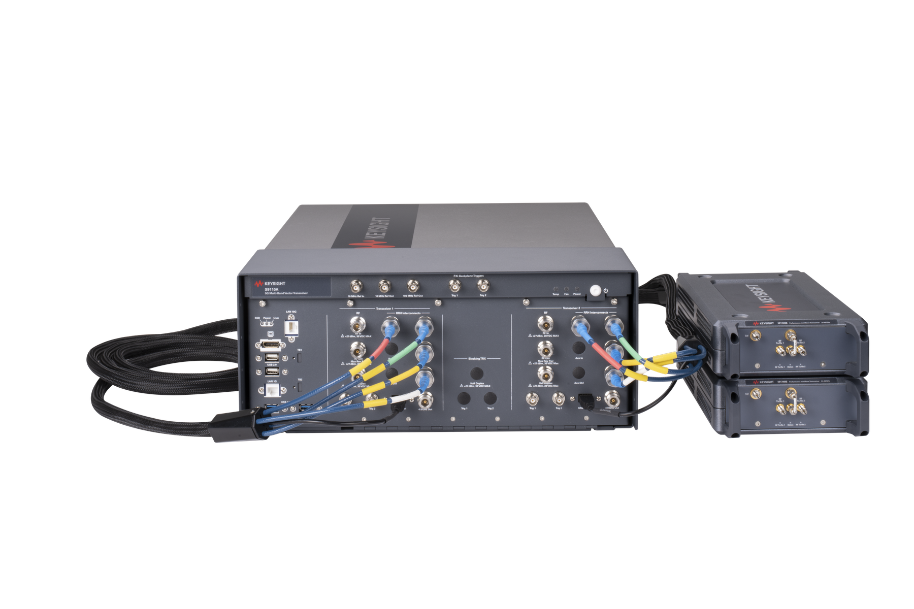
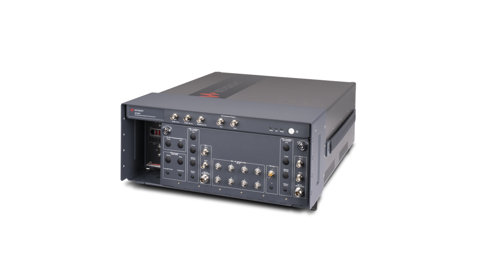
1. The illustration on this page depicts configuration with M1749B mmWave Transceiver. There may be differences in the front panel
• Keysight S9110A-TR1/TN1
5G Multi-Band Vector Transceiver, one channel
• Keysight S9110A-BK1
5G Multi-Band Vector Transceiver TR1 with Blocker
• Keysight S9110A-TR2/TN2
5G Multi-Band Vector Transceiver, two channels
• Option F32: μWave Transceiver Range
10-32 GHz
• Option F43: mmWave Transceiver Range
22.7-43.5 GHz
• Option F49: mmWave Transceiver Range
22.7-49.2 GHz
S9110A Connectors (Ports
1 to 6)
• All S9110A-TR1/TN1 and S9110A-BK1 standard configurations have μWave / mmWave ports on the
μWave / mmWave Transceiver that are RF Tx/Rx 1 and RF Tx/Rx
2
• All S9110A-TR1/TN1 standard configurations have RF Transceiver RF ports RF Out and RF In
• All S9110A-BK1 standard configurations have RF Transceiver RF ports RF Out and RF In
Although output and input ports RF Out and RF In with a Blocker on an S9110A-BK1 have the
same name on the external labeling as ports RF Out and RF In without a Blocker on an S9110A-
TR1, they have different system performance.
The differences are because the S9110A-BK1 has different source system performance than an
S9110A-TR1/TN1. On an S9110A-BK1, the Transmit (Tx) RF Out
380 MHz to 6 GHz, signal path is
routed through a hybrid combiner with additional cabling and switching that combines the RF Out of a
Primary Transceiver (M9410A PXIe VXT), “Wanted” signal, with the RF Out of a Secondary Transceiver
(M9410A PXIe VXT), “Blocker” signal.
The RF In path is not affected by the Blocker on an S9110A-BK1.
• All S9110A-TR2/TN2 standard configurations have two sets of μWave / mmWave ports and two sets RF
ports: o M1742A/M1749B μWave / mmWave Transceiver 1 has ports RF Tx/Rx 1 and RF Tx/Rx 2 o RF Transceiver 1 has ports RF Out and RF In o M1742A/M1749B μWave / mmWave Transceiver 2 has ports RF Tx/Rx 1 and RF Tx/Rx
2
- RF Transceiver
2 has ports RF Out and RF In
Figure 1. S9110A-TR1/TN1 (with F32, F43 or F49 options) 5G Multi-Band Vector Transceiver configuration
1
Figure 2. S9110A-BK1 (with F43 or F49 options)
5G Multi-Band Vector Transceiver TR1 with Blocker configuration
and rear panel connectors of M1742A. For accurate information regarding the illustration of M1742A and M1749B, refer to S9110A
条件:1. The illustration on this page depicts configuration with M1749B mmWave Transceiver. There may be differences in the front panel
Figure 3. S9110A-TR2/TN2 (with F32, F43 or F49 options) 5G Multi-Band Vector Transceiver configuration
1
and rear panel connectors of M1742A. For accurate information regarding the illustration of M1742A and M1749B, refer to S9110A
When working with M1749B, the following specs reflect the F49 Option. For the F43 option all instances of
49.2 GHz are limited to 43.5 GHz.
M1742A μWave connectors
RF Tx/Rx 1 and RF Tx/Rx
2
10 to 32 GHz, settable
M1749B mmWave connectors
RF Tx/Rx 1 and RF Tx/Rx
2
22.7 to 49.2 GHz, settable
All S9110A standard configurations
RF Transceiver connectors
RF In or RF In
380 to 6000 MHz
条件:Center Frequency Maximum Bandwidth (Nominal)
M1742A μWave connectors
RF Tx/Rx 1 and RF Tx/Rx
2
10 to 10.6 GHz (Center frequency – 10000 MHz) x
2 MHz
31.4 to 32 GHz (32000 MHz – Center frequency) x
2 MHz
M1749B mmWave connectors
RF Tx/Rx 1 and RF Tx/Rx
2
All S9110A Standard Configurations
RF Transceiver Connectors
RF In or RF In 380 to 550 MHz 100 MHz 550 to 1310 MHz 200 MHz 1310 to 2000 MHz
600 MHz
5480 to 6000 MHz (6080 MHz – Center frequency) x
2 MHz
M1742A μWave connectors
RF Tx/Rx 1 and RF Tx/Rx
2
10 to 32 GHz -100 dBm to +100 dBm
1
M1749B mmWave connectors
RF Tx/Rx 1 and RF Tx/Rx
2
22.7 GHz - 49.2 GHz -100 dBm to +100 dBm
1
All S9110A standard configurations
RF Transceiver connectors
条件:“RF Tx / Rx 1 and RF Tx / Rx 2” section of M1742A and M1749B on page 18, 19.
RF In or RF In 380 to 6000 MHz
-150 dBm to +27 dBm
Half duplex connector (Option HD1, HD2) 380 to 6000 MHz -150 dBm to +27 dBm 1. This is settable input range in instrument software. For actual maximum allowed input level, refer to “Amplitude” specification of
Absolute Amplitude Accuracy (CW Mode)
20 to 35 °C
Frequency Range Level Accuracy 10 to 20 GHz –50 dBm to 0 dBm ≤ ± 1.55 dB, ± 0.70 dB typical 20 to 32 GHz –50 dBm to 0 dBm ≤ ± 1.85 dB, ± 0.95 dB typical 25
± 3 °C
Frequency Range Level Accuracy 22.7 to 43.5 GHz –50 dBm to –10 dBm ≤ ± 1.90 dB
± 1.20 dB typical
–10 dBm to –5 dBm ≤ ±1.95 dB
± 1.20 dB typical
43.5 to 49.2 GHz –50 dBm to –10 dBm ≤ ± 2.15 dB
± 1.35 dB typical
–10 dBm to –5 dBm ≤ ± 2.05 dB
± 1.30 dB typical
All S9110A standard
条件:Frequency Range Level Accuracy (nominal) 380 to 680 MHz –70 to +27 dBm ≤ ± 0.45 dB 680 to 910 MHz –70 to –8 dBm ≤ ± 0.45 dB
910 to 1310 MHz –70 to –8 dBm ≤
± 0.55 dB
1310 to 2000 MHz –70 to –30 dBm ≤
± 0.6 dB
–30 to +27 dBm ≤
± 0.65 dB
2000 to 3500 MHz –70 to –30 dBm ≤
± 0.7dB
3500 to 4500 MHz –70 to –30 dBm ≤
± 0.65 dB
4500 to 5400 MHz –70 to –30 dBm ≤
± 0.90 dB
5400 to 6000 MHz –70 to –30 dBm ≤
± 1.20 dB
Half duplex connector (Option HD1, HD2,
条件:Frequency Range Level Accuracy (Nominal) 380 to 910 MHz –70 to –30 dBm ≤ ± 0.5 dB
910 to 1310 MHz –70 to –30 dBm ≤
± 0.60 dB
1310 to 3500 MHz –70 to –30 dBm ≤
± 0.75 dB
3500 to 4500 MHz –70 to –30 dBm ≤
± 0.50 dB
–30 to +27 dBm ≤
± 0.80 dB
4500 to 5400 MHz –70 to –30 dBm ≤
± 1.15 dB
5400 to 6000 MHz –70 to –30 dBm ≤
±1.35 dB
Linearity (CW Mode) (Reference Power Level is
–5 dBm)
条件:Frequency Range Input Level Linearity (Nominal) 10 to 32 GHz –50 to –10 dBm ≤ ± 1.0 dB
条件:Frequency Range Input Level Linearity (Nominal) 24.0 to 49.2 GHz –50 to –20 dBm ≤ ± 1.0 dB
条件:Frequency Range Input Level Scale Fidelity (Nominal) 10 to 32 GHz –50 to –40 dBm ≤ ± 0.5 dB
条件:Frequency Range Input Level Scale Fidelity (Nominal) 24.0 to 49.2 GHz –50 to –40 dBm ≤ ± 0.6 dB
条件:M1742A: The center frequency can be set > than 31.4 GHz, but bandwidth will be reduced as 32 GHz is approached.
M1749B: The center frequency can be set > than 48.6 GHz, but bandwidth will be reduced as
49.2 GHz is
10.6 to 31.4 GHz 1200 MHz
± 1.0 dB
22.7 to 24.2 GHz 100 MHz
± 1.25 dB
24.2 to 24.3 GHz 800 MHz
± 1.25 dB
24.3 to 48.6 GHz 1200 MHz
± 1.25 dB
All S9110A standard
条件:Frequency Range Bandwidth Flatness (Nominal) 380 to 6000 MHz 100 MHz ± 1.1 dB 200 MHz ± 1.35 dB 400 MHz ± 1.25 dB
Test signal: FR1: 5G NR, 30 kHz subcarrier spacing
256 QAM
Test signal: FR2: 5G NR, 120 kHz subcarrier spacing
256 QAM
条件:Frequency Range 10.6 to 31.4 GHz EVM (Nominal)
100 MHz BW ≤ –37 dB
–40 to –30 dBm input power
≤ –45 dB
–30 to 0 dBm input power
400 MHz BW ≤ –32 dB
–40 to –30 dBm input power
≤ –40 dB
–30 to –20 dBm input power
≤ –44 dB
–20 to 0 dBm input power
8 x 100 MHz ≤ –28 dB
–40 to –30 dBm input power
≤ –37 dB
–30 to –20 dBm input power
≤ –39 dB
–20 to 0 dBm input power
条件:Frequency Range 24.5 to 48.7 GHz EVM (Nominal)
100 MHz BW ≤ –37 dB
–40 to –30 dBm input power
≤ –43 dB
–30 to –5 dBm input power
400 MHz BW ≤ –32 dB
–40 to –25 dBm input power
≤ –42 dB
–25 to –5 dBm input power
8 x 100 MHz ≤ –30 dB
–40 to –25 dBm input power
≤ –42 dB
–25 to –5 dBm input power
All S9110A standard
FR1 (Sub
6 GHz) EVM (Nominal)
100 MHz BW signal at 5000 MHz <
0.3% at –10 dBm input power
M1742A μWave connectors
RF Tx/Rx 1 and RF Tx/Rx
2
条件:Frequency Range 10.6 to 31.4 GHz EVM (Nominal)
1000 MHz BW ≤ –27 dB
–40 to –35 dBm input power
≤ –32 dB
–35 to –30 dBm input power
≤ –36 dB
–30 to –25 dBm input power
≤ –39 dB
–25 to –20 dBm input power
≤ –41 dB
–20 to –15 dBm input power
≤ –42 dB
–15 to 0 dBm input power
Test signal: DVB–S2X
Equalizer filter length
51
EVM normalization reference: Reference RMS
M1742A μWave connectors
RF Tx/Rx 1 and RF Tx/Rx
2
条件:Frequency Range 10.6 to 31.4 GHz EVM (Nominal)
500 MHz BW ≤ –30 dB
–40 to –35 dBm input power
≤ –35 dB
–35 to –30 dBm input power
≤ –40 dB
–30 to –25 dBm input power
≤ –43 dB
–25 to –20 dBm input power
≤ –44 dB
–20 to 0 dBm input power
Adjacent Channel Leakage Ration (ACLR)
M1742A μWave connectors
RF Tx/Rx 1 and RF Tx/Rx
2
条件:Frequency Range 10.6 to 31.4 GHz ACLR (Nominal)
Frequency Range 22.7 to 48.6 GHz ACLR (Nominal)
100 MHz BW ≤ –51 dBc
–40 to 0 dBm input power
400 MHz BW ≤ –42 dBc
–40 to 0 dBm input power
8 x 100 MHz ≤ –40 dBc
–40 to 0 dBm input power
M1749B mmWave connectors
RF Tx/Rx 1 and RF Tx/Rx
2
100 MHz BW ≤ –43 dBc
–10 to –5 dBm input power
≤ –50 dBc
–30 to –10 dBm input power
≤ –47 dBc
–40 to –30 dBm input power
400 MHz BW ≤ –44 dBc
–30 to –5 dBm input power
≤ –41 dBc
–40 to –30 dBm input power
8 x 100 MHz ≤ –42 dBc
–30 to –5 dBm input power
≤ –37 dBc
–40 to –30 dBm input power
All S9110A standard configurations
FR1 (Sub
6 GHz) ACLR (Nominal)
100 MHz BW signal at 5000 MHz <
–63 dBc at 0 dBm input power
M1742A μWave connectors
RF Tx/Rx 1 and RF Tx/Rx
2
10 to 32 GHz, settable
M1749B mmWave connectors
RF Tx/Rx 1 and RF Tx/Rx
2
22.7 to 49.2 GHz, settable
All S9110A standard configurations RF
RF Out or RF Out
380 to 6000 MHz
条件:Center Frequency Maximum Bandwidth (Nominal)
Center Frequency Maximum Bandwidth (Nominal)
Center Frequency Maximum Bandwidth (Nominal)
M1742A μWave connectors
RF Tx/Rx 1 and RF Tx/Rx
2
10 to 10.6 GHz (Center frequency – 10000 MHz) x
2 MHz
31.4 to 32 GHz (32000 MHz – Center frequency) x
2 MHz
M1749B mmWave connectors
RF Tx/Rx 1 and RF Tx/Rx
2
All S9110A standard configurations
RF Transceiver connectors
RF Out or RF Out 380 to 550 MHz 100 MHz 550 to 1310 MHz 200 MHz 1310 to 2000 MHz
600 MHz
5480 to 6000 MHz (6080 MHz – Center frequency) x
2 MHz
M1742A μWave connectors
10 to 32 GHz CW
–70 dBm to +10 dBm
Modulated
–40 dBm to +5 dBm
M1742A μWave connectors
10 to 32 GHz CW
–70 dBm to +8 dBm
Modulated
–40 dBm to +3 dBm
M1749B mmWave connectors
RF Tx/Rx 1 and RF Tx/Rx
2
22.7 to 49.2 GHz CW
–70 dBm to +10 dBm
Modulated
–40 dBm to +5 dBm
S9110A option TR1 or TR2
RF transceiver connectors
RF Out 380 to 6000 MHz CW
–120 dBm to +20 dBm
Modulated: Depends on Crest Factor
S9110A option BK1
"wanted" signal
–120 dBm to +7 dBm
"Blocker: signal
–120 dBm to +2 dBm
Modulated: Depends on Crest Factor
Option HD1 (RFHD), HD2, HDB 380 to 6000 MHz CW
–120 dBm to +5 dBm
Frequency Range Level Accuracy
20 to 35°C
M1742A μWave connectors
RF Tx/Rx 1 and RF Tx/Rx
2
10 to 22 GHz –50 to 0 dBm ≤ ± 1.90 dB
± 0.85 dB typical
22 to 27 GHz –50 to 0 dBm ≤ ± 2.15 dB
± 1.05 dB typical
27 to 29 GHz –50 to 0 dBm ≤ ± 2.45 dB
± 1.30 dB typical
29 to 32 GHz –50 to 0 dBm ≤ ± 3.20 dB
± 1.80 dB typical
25±3°C
M1749B mmWave connectors
RF Tx/Rx 1 and RF Tx/Rx
2
22.7 to 43.5 GHz –50 to –10 dBm ≤ ± 2.20 dB
± 1.35 dB typical
–10 to –5 dBm ≤ ± 2.05 dB
± 1.30 dB typical
43.5 to 49.2 GHz –50 to –10 dBm ≤ ± 2.70 dB
± 1.75 dB typical
–10 to –5 dBm ≤ ± 2.25 dB
±1.40 dB typical
S9110A Option TR1 or TR2 RF
条件:Frequency Range Level Accuracy (Nominal) 380 to 550 MHz ≤ +20 to –80 dBm ≤ ± 0.55 dB
≤ –80 to –120 dBm ≤
± 0.80 dB
550 to 2000 MHz ≤ +20 to –15 dBm ≤
± 0.70 dB
≤ –15 to –80 dBm ≤
± 0.55 dB
≤ –80 to –110 dBm ≤
± 0.85 dB
2000 to 3900 MHz ≤ +20 to –15 dBm ≤
± 0.60 dB
≤ –15 to –80 dBm ≤
± 0.70 dB
≤ –80 to –110 dBm ≤
± 1.30 dB
3900 to 5700 MHz ≤ +20 to –15 dBm ≤
± 0.80 dB
≤ –15 to –80 dBm ≤
± 1.10 dB
≤ –80 to –100 dBm ≤
± 1.20 dB
5700 to 6000 MHz ≤ +20 to –15 dBm ≤
± 0.80 dB
≤ –15 to –80 dBm ≤
± 1.10 dB
≤ –80 to –90 dBm ≤
± 1.20 dB
S9110A Option BK1 RF transceiver
Primary transceiver, “Wanted” signal 380 to 550 MHz ≤ +17 to –83 dBm ≤
± 0.55 dB
≤ –83 to –120 dBm ≤
± 0.80 dB
550 to 2000 MHz ≤ +17 to –18 dBm ≤
± 0.70 dB
≤ –18 to –83 dBm ≤
± 0.55 dB
≤ –83 to –113 dBm ≤
± 0.85 dB
2000 to 3900 MHz ≤ +17 to –18 dBm ≤
± 0.60 dB
≤ –18 to –83 dBm ≤
± 0.70 dB
≤ –83 to –113 dBm ≤
± 1.30 dB
3900 to 5700 MHz ≤ +17 to –18 dBm ≤
± 0.80 dB
≤ –18 to –83 dBm ≤
± 1.10 dB
≤ –83 to –103 dBm ≤
± 1.20 dB
5700 to 6000 MHz ≤ +17 to –18 dBm ≤
± 0.80 dB
≤ –18 to –83 dBm ≤
± 1.10 dB
≤ –83 to –93 dBm ≤
± 1.20 dB
S9110A Option BK1 RF
条件:Frequency Range Level Accuracy (Nominal) 380 to 550 MHz ≤ +5 to –80 dBm ≤ ± 0.50 dB
Frequency Range Input Level Linearity (Nominal)
Secondary transceiver, “Blocker” signal 380 to 550 MHz ≤ +2 to –98 dBm ≤
± 0.55 dB
≤ –98 to –120 dBm ≤
± 0.80 dB
550 to 2000 MHz ≤ +2 to –33 dBm ≤
± 0.70 dB
≤ –33 to –98 dBm ≤
± 0.55 dB
≤ –98 to –120 dBm ≤
± 0.85 dB
2000 to 3900 MHz ≤ +2 to –33 dBm ≤
± 0.60 dB
≤ –33 to –98 dBm ≤
± 0.70 dB
≤ –98 to –120 dBm ≤
± 1.30 dB
3900 to 5700 MHz ≤ +2 to –33 dBm ≤
± 0.80 dB
≤ –33 to –98 dBm ≤
± 1.10 dB
≤ –98 to –118 dBm ≤
± 1.20 dB
5700 to 6000 MHz ≤ +2 to –33 dBm ≤
± 0.80 dB
≤ –33 to –98 dBm ≤
± 1.10 dB
≤ –98 to –108 dBm ≤
± 1.20 dB
Half duplex connector (Option HD1, HD2, HDB)
≤ –80 to –90 dBm ≤
± 0.65 dB
550 to 2000 MHz ≤ +5 to –15 dBm ≤
± 0.55 dB
≤ –15 to –80 dBm ≤
± 0.60 dB
≤ –80 to –90 dBm ≤
± 0.75 dB
2000 to 3900 MHz ≤ +5 to –15 dBm ≤
± 0.50 dB
≤ –15 to –80 dBm ≤
± 0.80 dB
≤ –80 to –90 dBm ≤
± 1.10 dB
3900 to 6000 MHz ≤ +5 to –15 dBm ≤
± 0.90 dB
≤ –80 to –90 dBm ≤
± 1.25 dB
Linearity (CW Mode) (Reference Power Level is
–5 dBm)
M1742A μWave connectors
RF Tx/Rx 1 and RF Tx/Rx
2
10 to 32 GHz –50 to 0 dBm ≤
± 0.9 dB
M1749B mmWave connectors
RF Tx/Rx 1 and RF Tx/Rx
2
22.7 to 49.2 GHz –50 to –30 dBm ≤
± 1.5 dB
When working with M1749B, the center frequency can be set > than
48.6 GHz, but bandwidth will be reduced as
49.2 GHz is approached.
When working with M1742A, the center frequency can be set > than
31.4 GHz, but bandwidth will be reduced as
32 GHz is approached.
M1742A μWave connectors
RF Tx/Rx 1 and RF Tx/Rx
2
10.6 to 31.4 GHz 1200 MHz
± 1.2 dB
M1749B mmWave connectors
RF Tx/Rx 1 and RF Tx/Rx
2
24.3 to 48.6 GHz 1200 MHz
± 1.5 dB
All S9110A standard configurations
RF Transceiver connectors
RF Out or RF Out 380 to 6000 MHz 100 MHz ± 0.5 dB 200 MHz ± 0.8 dB 400 MHz
± 1.0 dB
Test signal for FR1: 5G NR, 30 kHz subcarrier spacing
256 QAM
Test signal for FR2: 5G NR, 120 kHz subcarrier spacing
256 QAM
M1742A μWave connectors
条件:Frequency Range 10.6 to 31.4 GHz EVM (Nominal)
Frequency Range 22.7 to 49.2 GHz EVM (Nominal)
100 MHz BW ≤ –37 dB
–40 to –30 dBm input power
≤ –45 dB
–30 to 0 dBm input power
400 MHz BW ≤ –32 dB
–40 to –30 dBm input power
≤ –40 dB
–30 to –20 dBm input power
≤ –44 dB
–20 to 0 dBm input power
8 x 100 MHz ≤ –28 dB
–40 to –30 dBm input power
≤ –37 dB
–30 to –20 dBm input power
≤ –39 dB
–20 to 0 dBm input power
M1749B mmWave connectors
100 MHz BW ≤ –33 dB
–40 to –30 dBm input power
≤ –42 dB
–30 to –5 dBm input power
400 MHz BW ≤ –28 dB
–40 to –30 dBm input power
≤ –37 dB
–30 to –25 dBm input power
≤ –41 dB
–25 to –5 dBm input power
8 x 100 MHz ≤ –30 dB
–35 to –25 dBm input power
≤ –38 dB
–25 to –5 dBm input power
All S9110A standard
FR1 (Sub
6 GHz) EVM (Nominal)
100 MHz BW signal at 4000 MHz <
0.4% at –10 dBm output power
100 MHz BW signal at 5000 MHz <
0.6% at –10 dBm output power
M1742A μWave connectors
条件:Frequency Range 10.6 to 31.4 GHz EVM (Nominal)
1000 MHz ≤ –27 dB
–40 to –35 dBm input power
≤ –32 dB
–35 to –30 dBm input power
≤ –36 dB
–30 to –25 dBm input power
≤ –39 dB
–25 to –20 dBm input power
≤ –41 dB
–20 to –15 dBm input power
≤ –42 dB
–15 to 0 dBm input power
Test Signal: DVB–S2X
Equalizer filter length
51
EVM Normalization Reference: Reference RMS
M1742A μWave connectors
条件:Frequency Range 10.6 to 31.4 GHz EVM (Nominal)
500 MHz ≤ –30 dB
–40 to –35 dBm input power
≤ –35 dB
–35 to –30 dBm input power
≤ –40 dB
–30 to –25 dBm input power
≤ –43 dB
–25 to –20 dBm input power
≤ –44 dB
–20 to 0 dBm input power
Adjacent Channel Leakage Ration (ACLR)
条件:Frequency Range 10.6 to 31.4 GHz ACLR (Nominal)
Frequency range 22.7 to 49.2 GHz ACLR (nominal)
Test signal for FR1: 5G NR, 30 kHz subcarrier spacing
256 QAM
Test signal for FR2: 5G NR, 120 kHz subcarrier spacing
256 QAM
M1742A μWave connectors
Measured in loopback 100 MHz BW ≤ –51 dBc, –40 to 0 dBm input power 400 MHz BW ≤ –42 dBc, –40 to 0 dBm input power 8 x 100 MHz ≤ –40 dBc
–40 to 0 dBm input power
M1749B mmWave connectors
100 MHz BW ≤ –48 dBc
–25 to –5 dBm input power
≤ –43 dBc
–40 to –25 dBm input power
400 MHz BW ≤ –43 dBc
–30 to –5 dBm input power
≤ –42 dBc
–35 to –30 dBm input power
≤ –40 dBc
–40 to –35 dBm input power
8 x 100 MHz ≤ –37 dBc
–30 to –5 dBm input power
≤ –36 dBc
–40 to –30 dBm input power
All S9110A standard
Note: The S9110A–BK1
Primary Transceiver (M9410A
FR1 (Sub
6 GHz) ACLR (nominal)
100 MHz BW signal at 4000 MHz <
–57 dBc at 0 dBm input power
100 MHz BW signal at 5000 MHz <
–55 dBc at 0 dBm input power
S9110A
5G multi–band vector
Altitude up to 6,561.68 ft (2,000 m)
Operating temperature
15 to 35 °C maximum relative humidity (non–
S9110A base system (PXIe
chassis with modules, rugged panel, and cables) 100 / 120 V, 50 / 60 Hz 220 / 240 V
50 / 60 Hz
1200 W Max (lower range)
1300 W Max (upper range)
M1742A 120 VAC (via supplied
0950-6166
M1749B 120 VAC (via supplied
0950-6166
S9110A base system Height
197.8 mm (7.79 in); with feet installed
Width
449.5 mm (17.70 in); with rugged panel
Depth 568.9 mm (22.40 in); with rugged panel (from back bumper to front
M1742A Height
70 mm (2.76 in)
M1749B Height
70 mm (2.76 in)
S9101A rack space 2 x 2U x
1 rack width
S9110A–TR1/TN1 base system
20.4 kg (45.0 lbs)
S9110A–TR2/TN2 base system
22.6 kg (49.8 lbs)
S9110A–BK1 base system
24.0 kg (53.0 lbs)
Interface LAN RJ-45
The recommended calibration cycle is one year; calibration services are available through Keysight service
LAN, Display Port, and USB Connectors, M9038A
LAN
1 and LAN2 (TCP / IP Interface)
Connectors (Ethernet) One
10 / 100 / 1000 BASE–T (RJ–45)
One
100 / 1000 / 10 GB BASE–T (RJ–45)
Connectors (video) One, DisplayPort++
Connectors Two, USB
2.0 (Type A)
Connectors Two, USB
3.0 (Type A)
S9110A Base System Front Panel
条件:Accuracy ± 16 Hz, typical, within 1 year since last calibration, from 20 to 30°C.
Frequency Reference
100 MHz Ref Out and 10 MHz Ref In/Out Connectors Above the Rugged Front Panel
100 MHz Ref Out, Frequency Reference (If Available)
Refer to the Keysight M9300A PXIe Frequency Reference Data
Sheet · details 开精度, 老化率, 和稳定度
Recommended calibration cycle
1 year
条件:Accuracy ± 1.6 Hz, typical, within 1 year since last calibration, from 20 to 30°C.
Amplitude
9.5 dBm (nominal)
10 MHz Ref Out, Frequency Reference
Refer to the Keysight M9300A PXIe Frequency Reference Data
Sheet · details 开精度, 老化率, 和稳定度
Recommended calibration cycle
1 year
Amplitude
9.5 dBm (nominal)
10 MHz Ref In
Connects behind rugged panel to M9300A PXIe Reference Ref In and locks to another reference with a value from
1 to 110 MHz.
条件:Input amplitude 0 to 10 dBm (nominal)
Frequency
1 MHz to 110 MHz, sine wave
Lock range
± 1 ppm (nominal)
Trig 1 and Trig
2 Connectors Above the Rugged Front Panel
Connects behind rugged panel to M9019A PXIe Chassis Trig 1 and Trig
2. These two front panel trigger
connectors (Trig 1 and Trig 2) above the rugged front panel connect to the PXI [0:7] backplane trigger bus in the
M9019A chassis and can be configured as Input or Output.
Direction control Input or output (configurable)
Output level 3.3 V CMOS (TTL compatible
5 V tolerant)
Output impedance
50 Ω (typical)
Output trigger source PXI_Trig0 - PXI_Trig7 (Segment
2 or 3)
Input level 3.3 V CMOS (TTL compatible
5 V tolerant)
Input impedance
3 kΩ (typical)
Input trigger destination PXI_Trig0 - PXI_Trig7 (Segment
2 or 3)
Input threshold
1.65 V (typical)
Minimum swing
250 mV (typical)
Minimum pulse width
100 ns (typical)
Transceiver Connectors, RF
380 MHz to 6 GHz on the Rugged Front Panel
条件:Connector Type-N (f), 50 Ω (nominal)
Frequency range
380 MHz to 6 GHz
Amplitude 0 VDC
+27 dBm maximum safe input power
条件:Connector Type-N (f), 50 Ω (nominal)
Connector Type-N (f), 50 Ω (nominal)
Frequency range
380 MHz to 6 GHz
Amplitude 0 VDC
+30 dBm maximum applied reverse input power
Half duplex, Option HD1, HD2
Frequency range
380 MHz to 6 GHz
Amplitude 0 VDC
+30 dBm maximum safe input power
条件:Input impedance 1 kΩ or 50 Ω nominal
IF In, IF Out, and LO / Pwr / Ctrl Out connect to the M1742A or M1749B.
Input level Range
0 to +3.3V
Output impedance
50 Ω nominal
Output Level
+3.3V LVTTL, LVDS
Transceiver Connectors, Head μWave / mmWave
10 to 32 GHz or 22.7 to 49.2 GHz on the Rugged Front Panel
条件:Connector Type-N (f), 50 Ω (nominal)
Frequency range
380 MHz to 6 GHz
Amplitude ± 10 VDC
+33 dBm maximum
条件:Connector Type-N (f), 50 Ω (nominal)
Connector Type-N (f), 50 Ω (nominal)
Frequency range
380 MHz to 6 GHz
Amplitude ± 10 VDC
+33 dBm maximum
LO1 and LO2 Out
Frequency range
380 MHz to 6 GHz
条件:Connector Type-N (f), 50 Ω (nominal)
S9110A is only provided for the frequency bands called out in this Data Sheet.
Connector 2.4 mm (f), 50 Ω (nominal)
Connector USB
2.0 (Type A)
4.8 GHz Out (Not Used with F43 / F49 Options)
M1742A μWave Transceiver
Although the M1742A μWave Transceiver is operational from 10 to 32 GHz, the performance information for the
RF Tx / Rx 1 and RF Tx / Rx
2
These ports can be configured either to supply a μWave signal to a Device Under Test (DUT) or to
receive a μWave signal from a DUT
Amplitude 30 VDC
+25 dBm maximum input
Control (Not Used with S9110A)
条件:for the S9110A is only provided for the frequency bands called out in this Data Sheet.
Connector 2.4 mm (f), 50 Ω (nominal)
Connector
19 V DC power supply input
M1749B mmWave Transceiver
Although the M1749B mmWave Transceiver is operational from 22.7 to 49.2 GHz, the performance information
RF Tx / Rx 1 and RF Tx / Rx
2
These ports can be configured either to supply a mmWave signal to a Device Under Test (DUT) or to
receive a mmWave signal from a DUT
Amplitude 10 VDC
+10 dBm maximum input
9.6 GHz In
9.6 GHz Out
Control (Not Used with S9110A)
Connector
19 V DC power supply input
以上指标摘自厂家官方数据手册,完整定义、测试条件与保证值口径以手册为准。完整指标、测试条件与定义口径请见产品页「软件和手册 | 白皮书」栏目中的官方数据手册。
是德科技 | KEYSIGHT · onetest 仪器资源库



 客服










 粤公网安备44030902003758