 个人中心
个人中心IQ带宽:1GHz
频率范围:DC至500MHz
时钟初始精度:±200 × 10-9
4TX,4RX
ONETEST 欢迎您


IQ带宽:1GHz
频率范围:DC至500MHz
时钟初始精度:±200 × 10-9
4TX,4RX
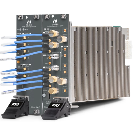
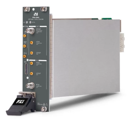
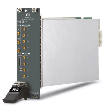
基带PXI矢量信号收发仪 - 500 MHz,1 GHz I/Q带宽
PXIe-5820是具有1 GHz复杂I/Q带宽的第二代矢量信号收发仪(VS)的基带型号。 它在单个2插槽PXI Express模块中结合了宽带I/Q数字转换器、宽带I/Q任意波形发生器和高性能用户可编程FPGA。 您可以使用VST进行各种应用,包括无线和蜂窝芯片组的基带I/Q测试;功率放大器数字预失真波形的包络跟踪;以及新的无线标准(如5G、802.11ax和LTE-Advanced Pro)的生成和分析。
产品编号: 783967-01
Complex I/Q equalized bandwidth[1] 1 GHz Frequency Range DC-500 MHz Initial adjustment accuracy ±200 × 10-9 Temperature stability ±1 × 10⁻⁶, maximum Aging ±1 × 10⁻⁶ per year, maximum Accuracy Initial adjustment accuracy ± Aging ± Temperature stabilityFrequency
NoteTo operate the device in complex baseband mode, configure each channel with identical ranges and termination. Complex baseband mode requires two input signals that are 90° out of phase.Internal Frequency Reference
| Common-Mode (V) | Accuracy (mV) at 23 °C | |
|---|---|---|
| -0.25 to 1.50 | ±2.5 | |
Conditions: Measured with a DMM. Common-mode offset is not adjusted during self-calibration. Valid for vertical ranges between 0.1 Vpp and 2.0 Vpp, differential. Measured with both input terminals terminated to ground through a high impedance >1 MΩ. | ||
| Reference Location | DC Offset at 23 °C ± 5 °C |
|---|---|
| At ADC | <-57 dBFS |
| At connector | <10 mV |
| Conditions: Terminated with 100 Ω differential impedance. | |
| Input Vertical Range (Vpp, Differential) | 23 °C ± 5 °C | 0 °C to 45 °C | |
|---|---|---|---|
| 0.5 to 4.0 | ±0.57 | ±0.71 | |
| ±0.15, typical | ±0.28, typical | ||
| 1.0 to 4.0 | ±0.44 | ±0.57 | |
Conditions: Valid for all common-mode voltages. Measured with 10 MHz CW tone from a 100 Ω differential source. This specification is valid only when the module is operating within the specified ambient temperature range and within ±5 °C from the last self-calibration temperature, as indicated by the niRFSA Device Temperature property or NIRFSA_ATTR_DEVICE_TEMPERATURE attribute. | |||
| Frequency | Input Vertical Range (Vpp, Differential) | 23 °C ± 5 °C | 0 °C to 45 °C |
|---|---|---|---|
| 100 kHz to 100 MHz | 0.5 to 4.0 | ±0.31, typical | ±0.36, typical |
| ±0.82 | ±0.92 | ||
| 1.0 to 4.0 | ±0.67 | ±0.77 | |
| 100 kHz to 250 MHz | 0.5 to 4.0 | ±0.31, typical | ±0.36, typical |
| ±0.82 | ±0.97 | ||
| 1.0 to 4.0 | ±0.67 | ±0.83 | |
| 100 kHz to 500 MHz | 0.5 to 4.0 | ±0.31, typical | ±0.62, typical |
| ±0.82 | ±1.22 | ||
| 1.0 to 4.0 | ±0.68 | ±1.10 | |
| 10 MHz to 250 MHz | 0.5 to 4.0 | ±0.10, typical | ±0.28, typical |
| ±0.25, typical | ±0.62, typical | ||
| 10 MHz to 500 MHz | |||
Conditions: Valid for all common-mode voltages. Referenced to 10 MHz. This specification is the individual I or Q channel flatness and is valid only when the module is operating within the specified ambient temperature range and within ±5 °C from the last self-calibration temperature, as indicated by the niRFSA Device Temperature property or the NIRFSA_ATTR_DEVICE_TEMPERATURE attribute. | |||

| Proximity to Final Settled Value (dB) | Settling Time (µs) |
|---|---|
| 0.5 | 9 |
| 0.1 | 100 |
| 0.05 | 100 |
| 0.01 | 100 |
Nominal common-mode voltage settling time (0.01 dB)[4] | 1.2 ms |
| Input Vertical Range (Vpp, Differential) | dBm/Hz | dBFs/Hz |
|---|---|---|
| 0.5 | -152 | -149 |
| 1 | -143 | -146 |
| 2 | -141 | -149 |
| 3 | -140 | -150 |
| Conditions: Terminated with a 100 Ω differential impedance. | ||


| Input Vertical Range (Vpp, Differential) | 10 MHz | 100 MHz | ||
|---|---|---|---|---|
| Typical | Nominal | Typical | Nominal | |
| 0.5 | -74 | -78 | -76 | -80 |
| 1 | -75 | -80 | -76 | -83 |
| 2 | -76 | -81 | -73 | -80 |
| 3 | -78 | -80 | -73 | -79 |
| Input Vertical Range (Vpp, Differential) | 10 MHz | 100 MHz | ||
|---|---|---|---|---|
| Typical | Nominal | Typical | Nominal | |
| 0.5 | -78 | -81 | -78 | -81 |
| 1 | -80 | -85 | -82 | -86 |
| 2 | -79 | -82 | -80 | -85 |
| 3 | -77 | -80 | -79 | -84 |
| Input Vertical Range (Vpp, Differential) | 10 MHz | 100 MHz | ||
|---|---|---|---|---|
| Typical | Nominal | Typical | Nominal | |
| 0.5 | -74 | -77 | -75 | -79 |
| 1 | -75 | -80 | -75 | -82 |
| 2 | -76 | -80 | -73 | -79 |
| 3 | -77 | -79 | -73 | -79 |
| Input Vertical Range (Vpp, Differential) | 10 MHz | 100 MHz | ||
|---|---|---|---|---|
| Typical | Nominal | Typical | Nominal | |
| 0.5 | -76 | -79 | -77 | -81 |
| 1 | -80 | -84 | -81 | -85 |
| 2 | -79 | -81 | -79 | -84 |
| 3 | -76 | -79 | -78 | -83 |
| Input Vertical Range (Vpp, Differential) | 10 MHz | 100 MHz |
|---|---|---|
| 0.5 | -89 | -89 |
| 1 | -89 | -88 |
| 2 | -89 | -89 |
| 3 | -89 | -88 |
| Input Vertical Range (Vpp, Differential) | 10 MHz | 100 MHz |
|---|---|---|
| 0.5 | -88 | -91 |
| 1 | -89 | -89 |
| 2 | -86 | -85 |
| 3 | -86 | -84 |
| Input Vertical Range (Vpp, Differential) | 10 MHz | 100 MHz | ||
|---|---|---|---|---|
| Typical | Nominal | Typical | Nominal | |
| 0.5 | -80 | -82 | -79 | -81 |
| 1 | -79 | -81 | -79 | -81 |
| 2 | -80 | -81 | -79 | -81 |
| 3 | -80 | -81 | -80 | -82 |
| Common-Mode (V) | Accuracy (mV) at 23 °C | |
|---|---|---|
| -0.25 to 1.50 | ±2 | |
Conditions: Measured with a DMM. Common-mode offset is not adjusted during self-calibration. Valid for vertical ranges between 0.1 Vpp and 2.0 Vpp, differential. Measured with both output terminals terminated to ground through a high impedance >1 MΩ. | ||
| Temperature Range | I/Q Output DC Offset Error |
|---|---|
| 23 °C ± 5 °C | -60 |
| dBr is dB relative to the peak to peak output voltage setting (Vpp, differential). | |
| Output Vertical Range (Vpp, Differential) | 23 °C ± 5 °C | 0 °C ± 45 °C | |
|---|---|---|---|
| 0.25 to 2.0 | ±0.43 | ±0.68 | |
| ±0.10, typical | ±0.35, typical | ||
Conditions: Valid for all common-mode voltages. 10 MHz CW tone into a 100 Ω differential load. This specification is valid only when the module is operating within the specified ambient temperature range and within ±5 °C from the last self-calibration temperature, as indicated by the niRFSG Device Temperature property or the NIRFSA_ATTR_DEVICE_TEMPERATURE attribute. | |||
| Frequency Range | Output Vertical Range (Vpp, Differential) | 23 °C ± 5 °C | 0 °C to 45 °C |
|---|---|---|---|
| 100 kHz to 100 MHz | 0.25 to 2.0 | ±0.17, typical | ±0.24, typical |
| ±0.51 | ±0.61 | ||
| 0.50 to 2.0 | ±0.44 | ±0.54 | |
| 100 kHz to 250 MHz | 0.25 to 2.0 | ±0.17, typical | ±0.25, typical |
| ±0.57 | ±0.69 | ||
| 0.50 to 2.0 | ±0.55 | ±0.68 | |
| 100 kHz to 500 MHz | 0.25 to 2.0 | ±0.18, typical | ±0.36, typical |
| ±0.65 | ±0.83 | ||
| 0.50 to 2.0 | ±0.59 | ±0.80 | |
Conditions: Valid for all common-mode voltages. Referenced to 10 MHz. This specification is the individual I or Q channel flatness and is valid only when the module is operating within the specified ambient temperature range and within ±5 °C from the last self-calibration temperature, as indicated by the niRFSG Device Temperature property or the NIRFSA_ATTR_DEVICE_TEMPERATURE attribute. | |||

| Proximity to Final Settled Value (dB) | Settling Time (us) |
|---|---|
| 0.5 | 9 |
| 0.1 | 100 |
| 0.05 | 100 |
| 0.01 | 100 |
Nominal common-mode settling time (0.01 dB)[11] | 1.2 ms |
| Output Vertical Range (Vpp, Differential) | dBm/Hz | dBFS/Hz |
|---|---|---|
| 0.5 | -152 | -147 |
| 1 | -154 | -155 |
| 2 | -156 | -162 |
| Conditions: Terminated with a 100 Ω differential impedance. | ||
| Output Vertical Range (Vpp, Differential) | 10 MHz | 100 MHz | ||
|---|---|---|---|---|
| Typical | Nominal | Typical | Nominal | |
| 0.5 | -77 | -80 | -70 | -74 |
| 1 | -78 | -80 | -69 | -74 |
| 2 | -69 | -71 | -66 | -68 |
| Output Vertical Range (Vpp, Differential) | 10 MHz | 100 MHz | ||
|---|---|---|---|---|
| Typical | Nominal | Typical | Nominal | |
| 0.5 | -75 | -78 | -69 | -73 |
| 1 | -77 | -78 | -69 | -73 |
| 2 | -69 | -70 | -65 | -67 |
| Output Vertical Range (Vpp, Differential) | 10 MHz | 100 MHz | ||
|---|---|---|---|---|
| Typical | Nominal | Typical | Nominal | |
| 0.5 | -72 | -82 | -67 | -77 |
| 1 | -73 | -81 | -68 | -77 |
| 2 | -74 | -82 | -66 | -76 |
| Output Vertical Range (Vpp, Differential) | 10 MHz | 100 MHz | ||
|---|---|---|---|---|
| Typical | Nominal | Typical | Nominal | |
| 0.5 | -73 | -81 | -69 | -78 |
| 1 | -79 | -85 | -73 | -80 |
| 2 | -72 | -75 | -65 | -71 |
| Output Vertical Range (Vpp, Differential) | 10 MHz | 100 MHz | ||
|---|---|---|---|---|
| Typical | Nominal | Typical | Nominal | |
| 0.5 | -76 | -77 | -75 | -77 |
| 1 | -79 | -81 | -79 | -81 |
| 2 | -80 | -82 | -79 | -81 |
| Complex Bandwidth | Image Suppression |
|---|---|
| 200 MHz | -69 |
| 1 GHz | -61 |
Image suppression is equivalent to or better than the specification at all frequency offsets within the specified bandwidth. | |
| Real Bandwidth (MHz) | Real SINAD | Real ENOB | Complex SINAD | Complex ENOB |
|---|---|---|---|---|
| 0.5 | 80.1 | 13.0 | 80.5 | 13.1 |
| 1 | 79.9 | 13.0 | 80.4 | 13.1 |
| 2.5 | 79.7 | 13.0 | 80.3 | 13.1 |
| 5 | 78.8 | 12.8 | 79.4 | 12.9 |
| 10 | 77.9 | 12.6 | 78.4 | 12.7 |
| 20 | 77.7 | 12.6 | 78.3 | 12.7 |
| 100 | 76.3 | 12.4 | 77.4 | 12.6 |
| 500 | 69.5 | 11.3 | 70.6 | 11.4 |
| Complex equalized bandwidth is the combined bandwidth of I and Q channels. | ||||
| Real Bandwidth (MHz) | Real SINAD | Real ENOB | Complex SINAD | Complex ENOB |
|---|---|---|---|---|
| 0.5 | 79.3 | 12.9 | 80.5 | 13.1 |
| 1 | 78.7 | 12.8 | 80.1 | 13.0 |
| 2.5 | 75.8 | 12.3 | 77.9 | 12.6 |
| 5 | 76.8 | 12.5 | 78.7 | 12.8 |
| 10 | 75.8 | 12.3 | 77.9 | 12.6 |
| 20 | 74.3 | 12.0 | 76.8 | 12.5 |
| 100 | 69.7 | 11.3 | 72.5 | 11.8 |
| 500 | 63.6 | 10.3 | 66.6 | 10.8 |
| Complex equalized bandwidth is the combined bandwidth of I and Q channels. | ||||
| Vertical Range (Vpp, Differential) | 0 °C to 45 °C | |
|---|---|---|
| Center Frequency (MHz) | ||
| 10 MHz | 100 MHz | |
| 0.25 | -77 | -77 |
| -77 | -77 | |
| 0.50 | ||
| 1.00 | -78 | -76 |
| 2.00 | -73 | -72 |
Conditions: Measured in loopback with two-tone stimulus, each tone is -8 dBFS with a 700 kHz spacing between the tones (equally spaced from the center frequency). IQ In and IQ Out ports are configured with the same Vertical Range and with 0 V common-mode. | ||


| Vertical Range (Vpp, Differential) | 0 °C to 45 °C | |
|---|---|---|
| Center Frequency (MHz) | ||
| 10 MHz | 100 MHz | |
| 0.25 | -74 | -68 |
| -73 | -67 | |
| 0.50 | ||
| 1.00 | -73 | -68 |
| 2.00 | -73 | -67 |
Conditions: Measured in loopback with two-tone stimulus, each tone is -8 dBFS with a 700 kHz spacing between the tones (equally spaced from the center frequency). IQ In and IQ Out ports are configured with the same Vertical Range and with 0 V common-mode. | ||


EVM (Bandwidth: 80 MHz)[19] | -50 dB, typical |

EVM (Bandwidth: 80 MHz)[20] | -50 dB, typical |
EVM (Bandwidth: 160 MHz)[21] | -50 dB, typical |


EVM (Bandwidth: 20 MHz) [22] | -58 dB, typical |

| Analog-to-digital converters (ADCs)I/Q data rate[23]19 kS/s to 1.25 GS/s | |
| Digital-to-analog converters (DACs)I/Q data rate[24]19 kS/s to 1.25 GS/s |
FPGA | Xilinx Virtex-7 X690T |
LUTs | 433,200 |
Flip-flops | 866,400 |
DSP48 slices | 3,600 |
Embedded block RAM | 52.9 Mbits |
Data transfers | DMA, interrupts, programmed I/O |
Number of DMA channels | 56 |
Memory size | 2 banks, 2 GB per bank |
Theoretical maximum data rate | 12 GB/s per bank |
Memory size | 2 MB |
Maximum data rate (read) | 31 MB/s |
Maximum data rate (write) | 29 MB/s |
Connectors | MMPX (female) |
Input coupling, per terminal | DC |
Input type | Differential |
Number of channels | 2 |
Input voltage range per I/Q input pin[25] (no damage) | -3 V to 5 V |
Common-mode range[26] | -0.25 V to 1.5 V |
Maximum vertical range | 4 Vpp, differential |
DC differential input impedance | 100 ± 10 Ω, typical |


Connectors | MMPX (female) |
Output coupling, per terminal | DC |
Output type | differential |
Number of channels | 2 |
Maximum voltage range per I/Q output pin (no damage) | Vcom ±3.5 V |
Common-mode range[27] | -0.25 V to 1.5 V |
| NI-RFSG Signal Bandwidth Setting (Complex) | Maximum Vertical Range | |
|---|---|---|
| ≤ 160 MHz | 3.4, nominal | |
| ≤ 1 GHz | 2, typical | |
| Conditions: Into a 100 Ω differential load. | ||
DC differential output impedance | 100 ± 10 Ω, typical |


Connector | MMPX (female) |
Frequency | 10 MHz |
Tolerance | ±10 × 10-6 |
Amplitude | 0.7 Vpk-pk to 3.3 Vpk-pk into 50 Ω, typical. |
Input impedance | 50 Ω, nominal |
Coupling | AC |
Connector | MMPX (female) |
Frequency | 10 MHz, nominal |
Amplitude | 1.65 Vpk-pk into 50 Ω, nominal |
Output impedance | 50 Ω, nominal |
Coupling | AC |
Connector | MMPX (female) |
Input impedance | 10 kΩ, nominal |
Output impedance | 50 Ω, nominal |
Maximum DC drive strength | 24 mA |
| Absolute maximum input range | -0.5 V to 5.5 V |
| VIL, maximum | 0.8 V |
| VIH, minimum | 2.0 V |
| VOL, maximum | 0.2 V with 100 μA load |
| VOH, minimum | 2.9 V with 100 μA load |
Connector | Molex Nano-Pitch I/O |
5.0 V Power | ±5%, 50 mA maximum, nominal |
| Signal | Type | Direction |
|---|---|---|
| MGT Tx± <3..0> | Xilinx Virtex-7 GTH | Output |
| MGT Rx± <3..0> | Xilinx Virtex-7 GTH | Input |
| MGT REF± | Differential | Input |
| DIO <1..0> | Single-ended | Bidirectional |
| DIO <7..2> | Single-ended | Bidirectional |
| 5.0 V | DC | Output |
| GND | Ground | — |
Data rate | 500 Mbps to 12 Gbps, nominal |
Number of Tx channels | 4 |
Number of Rx channels | 4 |
I/O AC coupling capacitor | 100 nF |
Minimum differential output voltage | 800 mVpk-pk into 100 Ω, nominal |
Conditions: transmitter output swing at maximum setting.
| ≤6.6 GB/s | 150 mVpk-pk to 2,000 mVpk-pk, nominal |
| >6.6 GB/s | 150 mVpk-pk to 1,250 mVpk-pk, nominal |
Differential input resistance | 100 Ω, nominal |
| Data Clock | 156.25 MHz |
| MGT REF± Input | 60 MHz to 820 MHz, nominal |
AC coupling capacitors | 100 nF |
Differential input resistance | 100 Ω, nominal |
Differential input Vpk-pk range | 350 mV to 2000 mV, nominal |
Absolute maximum input range | -1.25 V to 4.5 V |

| Voltage (VDC) | Typical Current (A) |
|---|---|
| +3.3 | 3.3 |
| +12 | 6.0 |
| Power is 83 W, typical. Consumption is from both PXI Express backplane power connectors. Conditions: Simultaneous generation and acquisition using NI-RFSG and NI-RFSA at 1.25 GS/s I/Q rate, 45 °C ambient temperature. Power consumption depends on FPGA image being used. | |
Interval | 1 year |
PXIe-5820 module | 3U, two slot, PXI Express module 4.1 cm × 13.0 cm × 21.6 cm1.6 in. × 5.1 in. × 8.5 in. |
Weight | 795 g (28.0 oz) |
Maximum altitude | 2,000 m (800 mbar) (at 25 °C ambient temperature) |
Pollution Degree | 2 |
Indoor use only.
Ambient temperature range | 0 °C to 45 °C |
Relative humidity range | 10% to 90%, noncondensing |
Ambient temperature range | -40 °C to 71 °C |
Relative humidity range | 5% to 95%, noncondensing |
Operating shock | 30 g peak, half-sine, 11 ms pulse |
| Random vibrationOperating5 Hz to 500 Hz, 0.3 grmsNonoperating5 Hz to 500 Hz, 2.4 grms | |
0条提问
X
提问
X
回答
发表口碑
© 2026 Onetest仪器资源库 All Rights Reserved 粤ICP备17028186号-2
 粤公网安备44030902003758