频率范围:5GHz至21/31.3/44GHz
1 GHz带宽
ONETEST 欢迎您


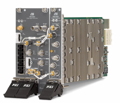
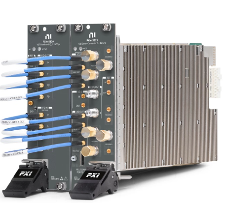

44 GHz,1 GHz带宽PXI矢量信号收发仪
PXIe-5831支持毫米波频段的验证和生产测试。PXIe-5831结合了一个矢量信号发生器、矢量信号分析仪、高速串行接口和基于FPGA的实时信号处理和控制。PXIe-5831结合了高速测量、生产测试仪器的小巧外形以及研发级台式仪器的灵活性和高性能,使其成为实验室和生产车间的理想解决方案。PXIe-5831可以满足5G新空口的严苛挑战,同时也能够测试各种蜂窝和无线标准,如Wi-Fi 6。此外,由于该仪器采用PXI Express结构,因而可轻松对系统进行扩展,以支持具有相位相干同步的多输入多输出(MIMO)配置。
产品编号: 786856-01 | 786853-01
PXIe-5831 IF 仪器 配置 包括 以下 模 块:
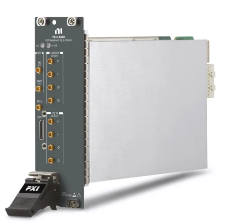
PXIe-5820 矢量信号收发器
PXIe-3622 矢量信号上/下变频器
PXIe-5831 中频和毫米波仪器配置包括以下模块:
PXIe-5820 矢量信号收发器
PXIe-3622 矢量信号上/下变频器
PXIe-5653 射频模拟信号发生器 (LO源)
一个或两个 mmRH-5582 毫米波射频头
Frequency bandwidth 1 GHz within the specified frequency ranges Tuning resolution[2] 4.45 uHz The LO2 frequency settling time includes the frequency lock time and settling time. Conditions: 20 kHz offset; module temperatures within ± 5 °C of last self-calibration temperature; LO2 LO Source: Onboard. Conditions: 20 kHz offset; module temperatures within ± 5 °C of last self-calibration temperature; LO1 LO Source: Onboard or Secondary.Frequency
NoteThe mmRH-5582 DIRECT TRX PORTS and SWITCHED TRX PORTS share the same frequency ranges and are only available on the PXIe-5831 mmWave instrument configurations.Frequency range[1]IF IN/OUT 0, IF IN/OUT 15 GHz to 21 GHzTRX ports (Transmit)22.5 GHz to 31.3 GHz37 GHz to 44 GHzTRX ports (Receive)22.5 GHz to 44 GHz Frequency Range Step Size Onboard Secondary 5 GHz to 14.2 GHz 2 MHz — >14.2 GHz to 21 GHz 4 MHz — 22.5 GHz to 44 GHz <1 Hz 8 MHz Frequency Settling Time
Frequency Step Size Frequency Lock Time (ms) ≤25 MHz 0.85 ≤50 MHz 1.10 ≤75 MHz 1.35 ≤80 MHz 1.35 ≤90 MHz 1.35 ≤100 MHz 1.35 ≤250 MHz 1.80 ≤500 MHz 6 ≤1.0 GHz 10 ≤2.0 GHz 13 ≤3.0 GHz 15 ≤5.1 GHz 17 NoteLO1 Frequency Tuning Time consists of the PXIe-5653 Lock Time + PXIe-5831 (LO1) Settling Time to Required Accuracy. The PXIe-5653 Lock Time is dependent on the RF Center Frequency (CF) frequency step change from initial frequency to final frequency. The relationship between the CF and the PXIe-5653 frequency is governed by the equation: F_PXIe-5653 = (FCF + FIF)/8. FIF is determined by the CF. For CF = 22.5 GHz to 31.3 GHz, FIF = 17.8 GHz; CF = >31.3 GHz to 40 GHz, FIF = 12 GHz; CF = >40 GHz to 44 GHz, FIF = 9 GHz For example, for a CF step change from 28 GHz to 39 GHz, first calculate the equivalent FPXIe-5653 for 28 GHz, which is 5.725 GHz, then the equivalent CF frequency for 39 GHz, which is 6.375 GHz. The PXIe-5653 step size is 6.375 GHz - 5.725 GHz = 650 MHz. The corresponding PXIe-5653 maximum frequency lock time is 10 ms. Settling Accuracy (Relative to Final Frequency) Settling Time (ms) Onboard* Secondary ≤1.0 × 10⁻⁶ 0.00 0.50 ≤0.1 × 10⁻⁶ 0.75 0.80 ≤0.01 × 10⁻⁶ 1.60 1.00 NoteIn Secondary mode, the LO1 frequency settling time includes the frequency lock time. In Onboard mode, the frequency lock time is defined in the previous table.* LO1 Frequency Tuning Time consists of the PXIe-5653 Lock Time + PXIe-5831 (LO1) Settling Time to Required Accuracy. The PXIe-5653 Lock Time is dependent on the RF Center Frequency (CF) frequency step change from initial frequency to final frequency. The relationship between the CF and the PXIe-5653 frequency is governed by the equation: F_PXIe-5653 = (FCF + FIF)/8. FIF is determined by the CF. For CF = 22.5 GHz to 31.3 GHz, FIF = 17.8 GHz; CF = >31.3 GHz to 40 GHz, FIF = 12 GHz; CF = >40 GHz to 44 GHz, FIF = 9 GHz For example, for a CF step change from 28 GHz to 39 GHz, first calculate the equivalent FPXIe-5653 for 28 GHz, which is 5.725 GHz, then the equivalent CF frequency for 39 GHz, which is 6.375 GHz. The PXIe-5653 step size is 6.375 GHz - 5.725 GHz = 650 MHz. The corresponding PXIe-5653 maximum frequency lock time is 10 ms. Settling Accuracy (Relative to Final Frequency) Settling Time (ms), Onboard 1.0 × 10⁻⁶ 0.50 0.1 × 10⁻⁶ 0.80 0.01 × 10⁻⁶ 1.00 Internal Frequency Reference
LO1 sourceOnboardInitial adjustment accuracy±50 × 10-9Temperature stability±50 × 10-9Aging±100 × 10-9 per yearAccuracyInitial adjustment accuracy ± Aging ± Temperature stabilitySecondaryInitial adjustment accuracy±5 × 10⁻⁶Temperature stability±1 × 10 -6, maximumAging±1 × 10⁻⁶ per year, maximumAccuracyInitial adjustment accuracy ± Aging ± Temperature stability LO2 source (Onboard)Initial adjustment accuracy±5 × 10⁻⁶Temperature stability±1 × 10 -6, maximumAging±1 × 10⁻⁶ per year, maximumAccuracyInitial adjustment accuracy ± Aging ± Temperature stability Spectral Purity
Frequency Phase Noise (dBc/Hz, Single Sideband) 5 GHz to 7.1 GHz -103 >7.1 GHz to 14.2 GHz -97 >14.2 GHz to 21 GHz -95 Frequency Phase Noise (dBc/Hz, Single Sideband) Onboard Secondary 22.5 GHz to 31.3 GHz -97 -86 >31.3 GHz to 40 GHz -99 -86 40 GHz to 44 GHz -103 -85 

Conditions: Valid over 23 °C ± 5 °C with the last self-calibration performed at 23°C. Measured with a tone 10 MHz offset from upconverter center frequency. For 0 °C to 45 °C, the leveled power specification output powers are 3 dB less than that of 23 °C ± 5 °C. Minimum output power Noise floor Output attenuator (analog power) resolution 1 dB, nominal Digital attenuation resolution[7] <0.1 dB <0.5 dB of final value 27 µs, nominal <0.1 dB of final value 40 µs, nominal Conditions: Peak power level -30 dBm to IF Output maximum leveled power specification; measured with a CW signal at 10 MHz offset from the configured upconverter center frequency; Upconverter/Downconverter Frequency Offset Mode: User-Defined; measurement performed after the PXIe-5831 has settled. This specification is valid only when the instrument is operating within the specified ambient temperature range and each module is within ±5 °C from the last self-calibration temperature, as measured with its onboard temperature sensors. Conditions: Peak power level -30 dBm to IF Output maximum leveled power specification; measured with a CW signal at I/Q center frequency, where I/Q center frequency is offset 257.5 MHz offset from the configured upconverter center frequency where the driver automatically applies a 257.5 MHz offset for signals with 450 MHz bandwidth or less. Upconverter/Downconverter Frequency Offset Mode: Enabled; measurement performed after the PXIe-5831 has settled. This specification is valid only when the instrument is operating within the specified ambient temperature range and each module is within ±5 °C from the last self-calibration temperature, as measured with its onboard temperature sensors. Conditions: Peak power level -30 dBm to IF Output maximum leveled power specification; measured with a CW signal at 10 MHz offset from the configured upconverter center frequency; Upconverter/Downconverter Frequency Offset Mode: User-Defined; measurement performed after the PXIe-5831 has settled. Relative accuracy describes the residual absolute accuracy error when compared to the absolute accuracy error at 0 dBm. This specification is valid only when the instrument is operating within the specified ambient temperature range and each module is within ±5 °C from the last self-calibration temperature, as measured with its onboard temperature sensors. Conditions: Peak power level -30 dBm to IF Output maximum leveled power specification; measured with a CW signal at I/Q center frequency, where I/Q center frequency is offset 257.5 MHz offset from the configured upconverter center frequency; Upconverter/Downconverter Frequency Offset Mode: Enabled; measurement performed after the PXIe-5831 has settled. Relative accuracy describes the residual absolute accuracy error when compared to the absolute accuracy error at 0 dBm. This specification is valid only when the instrument is operating within the specified ambient temperature range and each module is within ±5 °C from the last self-calibration temperature, as measured with the onboard temperature sensors. Conditions: Peak power level -30 dBm to IF Output maximum leveled power specification; module temperature within ±5 °C of last self-calibration temperature. Frequency response is defined as the maximum relative amplitude deviation from the reference offset frequency over the instantaneous bandwidth. For the PXIe-5831 IF output, the reference offset frequency is 10 MHz higher than the upconverter center frequency. For the absolute amplitude accuracy at the reference offset, refer to the IF Output Amplitude Accuracy section. Conditions: 10 averages; 40 dB baseband signal attenuation; noise measurement frequency offset by 200 MHz from the upconverter center frequency; the instrument driver is in peak mode. Measured on the PXIe-3622IF IN/OUT 1 port. The IF IN/OUT 0 port has a 1 dB to 5 dB degradation compared to the IF IN/OUT 1 port. Conditions: Measured by generating two -7 dBr tones at +95 MHz and +105 MHz off from the upconverter center frequency. The nominal peak envelope power is 1 dB below the Output Power Level Setting; the instrument driver is in peak mode. Conditions: Peak power level 0 dBm; measured with a CW signal at 100 MHz offset from the configured upconverter center frequency; Upconverter/Downconverter Frequency Offset Mode: User-Defined; measurement performed after the PXIe-5831 has settled. Includes CW and LO harmonics. Measured at 23 °C ambient within ±5 °C from the last self-calibration temperature. Conditions: Measured relative to a 0 dBm output tone. The maximum offset is limited to the instantaneous 1 GHz bandwidth at the referenced upconverter center frequency. Conditions: Measured relative to a 0 dBm output tone. Conditions: Peak output power levels -30 dBm up to the IF Output maximum leveled power specifications. The transmit output tone power at a maximum of -3 dBr. LO2 LO Source property set to Onboard. Conditions: Peak output power levels -30 dBm up to the IF Output maximum leveled power specifications. Output tone power at a maximum of -3 dBr. LO2 LO Source property set to Onboard. This specification describes the maximum residual sideband image within the 1 GHz device instantaneous bandwidth. Conditions: Valid over 23 °C ± 5 °C. Measured with a tone 10 MHz offset from upconverter center frequency. Minimum Output Power Noise Floor Output attenuator (analog power) resolution 1 dB, nominal Digital attenuation resolution[9] <0.1 dB <0.5 dB of final value 31 µs, nominal <0.1 dB of final value 43 µs, nominal Conditions: Valid for RF output power levels from -40 dBm up to the RF Output maximum leveled power specifications for direct and switched ports; measured with a CW signal at 10 MHz offset from the configured upconverter center frequency; Upconverter/Downconverter Frequency Offset Mode: User- Defined; measurement performed after the PXIe-5831 has settled. This specification is valid over 23 °C ± 5 °C with the last self-calibration performed at 23°C. Conditions: Valid for RF output power levels from -40 dBm up to the RF Output maximum leveled power specifications for direct and switched ports; measured with a CW signal at I/Q center frequency, where I/Q center frequency is offset 257.5 MHz offset from the configured upconverter center frequency where the driver automatically applies a 257.5 MHz offset for signals with 450 MHz bandwidth or less; Upconverter/Downconverter Frequency Offset Mode: Enabled; measurement performed after the PXIe-5831 has settled. This specification is valid over 23 °C ± 5 °C with the last self-calibration performed at 23°C. Conditions: Valid for RF output power levels from -40 dBm up to the RF Output maximum leveled power specifications for direct and switched ports; measured with a CW signal at 10 MHz offset from the configured upconverter center frequency; Upconverter/Downconverter Frequency Offset Mode: User- Defined; measurement performed after the PXIe-5831 has settled. Relative accuracy describes the residual absolute accuracy error when compared to the absolute accuracy error at 0 dBm. This specification is valid only when the instrument is operating within the specified ambient temperature range and each module is within ±5 °C from the last self-calibration temperature, as measured with its onboard temperature sensors. Conditions: Valid for RF output power levels from -40 dBm up to the RF Output maximum leveled power specifications for direct and switched ports; ; measured with a CW signal at I/Q center frequency, where I/Q center frequency is offset 257.5 MHz offset from the configured upconverter center frequency; Upconverter/Downconverter Frequency Offset Mode: Enabled; measurement performed after the PXIe-5831 has settled. Relative accuracy describes the residual absolute accuracy error when compared to the absolute accuracy error at 0 dBm. This specification is valid only when the instrument is operating within the specified ambient temperature range and each module is within ±5 °C from the last self-calibration temperature, as measured with its onboard temperature sensors. Conditions: Valid for RF output power levels from -35 dBm up to the RF Output maximum leveled power specifications for direct and switched ports. This specification is valid only when the instrument is operating within the specified ambient temperature range and each module is within ±5 °C from the last self-calibration temperature, as measured with its onboard temperature sensors. Frequency response is defined as the maximum relative amplitude deviation from the reference offset frequency. For the PXIe-5831 RF output, the reference offset frequency is 10 MHz higher than the upconverter center frequency over the instantaneous bandwidth. For the absolute amplitude accuracy at the reference offset, refer to the RF Output Amplitude Accuracy section. Conditions: Measured at both switched and direct TRX ports, +10 dBm valid for direct TRX ports only; 30 averages; 40 dB baseband signal attenuation; noise measurement frequency offset 200 MHz relative to the upconverter center frequency. The instrument driver is in peak mode. Conditions: Measured by generating two -7 dBr tones applied at +95 MHz and +105 MHz offset from the upconverter center frequency. The nominal peak envelope is 1 dB below the Output Power Level Setting; the instrument driver is in peak mode. Conditions: Measured by generating two -7 dBr tones applied at +95 MHz and +105 MHz offset from the upconverter center frequency. The nominal peak envelope is 1 dB below the Output Power Level Setting; the instrument driver is in peak mode. For >37 GHz, +5 dBm is outside the leveled power range and was not measured. Conditions: Peak output power levels -30 dBm up to the RF Output maximum leveled power specifications for direct and switched ports. The transmit tone power at a maximum of -3 dBr. LO1 and LO2 LO Source property set to Onboard. The values are with respect to the peak power level setting, hence dBr. Conditions: Peak output power levels -30 dBm up to the RF Output maximum leveled power specifications for direct and switched ports. The transmit tone power at a maximum of -3 dBr. LO1 and LO2 LO Source property set to Onboard. This specification describes the maximum residual sideband image within the 1 GHz device instantaneous bandwidth. Conditions: 23 °C; peak output power is set to within -40 dBm to the RF output maximum leveled power specification for direct and switched TRX ports. LO1 x 2 refers to out-of-band leakage where an LO1 harmonic product appears at the TRX port output as a function of the configured peak power level (hence dBr units), and upconverter center frequency (UCF). The relationship between the UCF frequency and the LO1 x 2 frequency is governed by the equation: FLO1x2 =(FUCF+FIF)/2. FIF is determined by the UCF. For UCF = 22.5 GHz to 31.3 GHz, FIF = 17.8 GHz; UCF > 31.3 GHz to 40 GHz, FIF = 12 GHz; UCF >40.0 GHz to 44 GHz, FIF = 9 GHz. In the frequency range 22.5 GHz to 31.3 GHz, the minimum frequency for FLO1x2 is when CF = 22.5 GHz and here FLO1x2 = 20.15 GHz; the maximum frequency for FLO1X2 is when CF = 31.3 GHz and there FLO1x2 = 24.55 GHz. In all cases, LO1x2 is out-of-band. The in-band residual spurs are a function of the transmit tone power (hence dBc units) and are measured to within the instantaneous 1 GHz bandwidth. This does not include carrier leakage and residual image. The out-of-band spur numbers refer to spurs that are offset from the upconverter center frequency between 500 MHz to 5 GHz away, but does not include the LO1 x 2. These spurs are a function of the transmit tone power and hence have dBc units. The RF Output power is set to +10 dBm. Includes CW harmonics only. For >37 GHz, the 3rd harmonic frequency is >110 GHz and outside the measured range. Amplitude range Average noise level to +20 dBm (CW RMS) Gain resolution 1 dB, nominal <0.5 dB of final value 27 µs, nominal <0.1 dB of final value 40 µs, nominal Conditions: Reference level -30 dBm to 0 dBm for specification; -30 dBm to 20 dBm for typical; measured with a CW signal at 10 MHz offset from the configured downconverter center frequency when a user-defined frequency offset is not applied; Upconverter/Downconverter Frequency Offset Mode: User-Defined; measurement performed after the PXIe-5831 has settled. This specification is valid only when the instrument is operating within the specified ambient temperature range and each module is within ±5 °C from the last self-calibration temperature, as measured with the onboard temperature sensors. Conditions: Reference level -30 dBm to 0 dBm for specification; -30 dBm to 20 dBm for typical; measured with a CW signal at the I/Q center frequency, where the I/Q center frequency is 257.5 MHz offset from the configured downconverter center frequency where the driver automatically applies a 257.5 MHz offset for signals with 450 MHz bandwidth and less; Upconverter/Downconverter Frequency Offset Mode: Enabled; measurement performed after the PXIe-5831 has settled. This specification is valid only when the instrument is operating within the specified ambient temperature range and each module is within ±5 °C from the last self-calibration temperature, as measured with the onboard temperature sensors. Conditions: Reference level -30 dBm to +20 dBm; measured with a CW signal at 10 MHz offset from the configured downconverter center frequency; Upconverter/Downconverter Frequency Offset Mode: User-Defined; measurement performed after the PXIe-5831 has settled. Relative accuracy describes the residual absolute accuracy error when compared to the absolute accuracy at 0 dBm. This specification is valid only when the instrument is operating within the specified ambient temperature range and each module is within ±5 °C from the last self-calibration temperature, as measured with the onboard temperature sensors. Conditions: Reference level -30 dBm to +20 dBm; measured with a CW signal at ±257.5 MHz offset from the configured downconverter center frequency where the driver automatically applies at the I/Q center frequency, where the I/Q center frequency is 257.5 MHz offset for signals with 450 MHz bandwidth and less; Upconverter/Downconverter Frequency Offset Mode: Enabled; measurement performed after the PXIe-5831 has settled. Relative accuracy describes the residual absolute accuracy error when compared to the absolute accuracy at 0 dBm. This specification is valid only when the instrument is operating within the specified ambient temperature range and each module is within ±5 °C from the last self-calibration temperature, as measured with the onboard temperature sensors. Conditions: Reference level -30 dBm to 0 dBm for specification; -30 dBm to 20 dBm for typical; module temperatures within ±5 °C of last self-calibration temperature. Frequency response is defined as the maximum relative amplitude deviation from the reference offset frequency over the instantaneous bandwidth. For the PXIe-5831 IF input, the reference offset frequency is 10 MHz higher than the downconverter center frequency. For the absolute amplitude accuracy at the reference offset, refer to the IF Input Amplitude Accuracy section. Conditions: Input terminated with a 50 Ω load; 10 averages; noise measurement frequency offset by 6 MHz from the downconverter center frequency. Measured on the PXIe-3622IF IN/OUT 1 port. The IF IN/OUT 0 port has a 2 dB degradation compared to the IF IN/OUT 1 port. Conditions: Measured with two -6 dBr tones applied at +95 MHz and +105 MHz offset from the downconverter center frequency. Conditions : Reference level 0 dBm. Measured with the IF IN 1 port terminated with 50 Ω. The maximum offset is limited to the instantaneous bandwidth at the referenced downconverter center frequency. Conditions: Reference level is -30 dBm to +15 dBm. Input tone power at a maximum of -3 dBr. LO2 LO Source property set to Onboard. Conditions: Reference Level is -30 dBm to +15 dBm. LO2 LO Source property set to Onboard. This specification describes the maximum residual sideband image within the 1 GHz device instantaneous bandwidth. Amplitude range Average noise level to +30 dBm (CW RMS) RF gain resolution 1 dB, nominal <0.5 dB of final value 31 µs, nominal <0.1 dB of final value 43 µs, nominal Conditions: Measured with a CW signal at 10 MHz offset from the configured downconverter center frequency; Upconverter/Downconverter Frequency Offset Mode: User-Defined; measurement performed after the PXIe-5831 has settled. This specification is valid only when the instrument is operating within 23 °C ± 5 °C ambient temperature range and each module is within ±5 °C from the last self-calibration temperature, as measured with its onboard temperature sensors. Conditions: Measured with a CW signal at 10 MHz offset from the configured downconverter center frequency; measurement performed after the PXIe-5831 has settled; Upconverter/Downconverter Frequency Offset Mode: User-Defined. This specification is valid only when the instrument is operating within 23 °C ± 5 °C ambient temperature range and within ±5 °C from the last self-calibration temperature, as measured with the onboard temperature sensors. Conditions: Reference level -30 dBm to +30 dBm; measured with a CW signal at 10 MHz offset from the configured downconverter center frequency; Downconverter Frequency Offset Mode: User-Defined; measurement performed after the PXIe-5831 has settled. Relative accuracy describes the residual absolute accuracy error when compared to the absolute accuracy at 0 dBm. This specification is valid over 23 °C ± 5 °C with the last self-calibration performed at 23 °C. Conditions: Valid for reference level -30 dBm to +30 dBm; measured with a CW signal at the I/Q center frequency, where the I/Q center frequency is257.5 MHz offset from the configured downconverter center frequency where the driver automatically applies a 257.5 MHz offset for signals with 450 MHz bandwidth and less; Upconverter/Downconverter Frequency Offset Mode: Enabled; measurement performed after the PXIe-5831 has settled. This specification is valid over 23 °C ± 5 °C with the last self-calibration performed at 23 °C. Conditions: Reference level -30 dBm to +30 dBm; measured with a CW signal at the I/Q center frequency, where the I/Q center frequency is 257.5 MHz offset from the configured downconverter center frequency where the driver automatically applies a 257.5 MHz offset for signals with 450 MHz bandwidth and less; Downconverter Frequency Offset Mode: Enabled; measurement performed after the PXIe-5831 has settled. Relative accuracy describes the residual absolute accuracy error when compared to the absolute accuracy at 0 dBm. This specification is valid over 23 °C ± 5 °C with the last self-calibration performed at 23 °C. Conditions: Valid over 23 °C ± 5 °C with self-calibration at 23 °C; for Direct and Switched TRX ports; input reference level -30 dBm to 0 dBm for specification; -30 dBm to 30 dBm for typical. Frequency response is defined as the maximum relative amplitude deviation from the reference offset frequency over the instantanous bandwidth. For the PXIe-5831 RF input, the reference offset frequency is 10 MHz higher than the downconverter center frequency. For the absolute amplitude accuracy at the reference offset, refer to the RF Input Amplitude Accuracy section. Conditions: Input terminated with a 50 Ω load; 30 averages; 40 dB baseband signal attenuation; noise measurement frequency offset by 6 MHz from the downconverter center frequency. Conditions: Measured by generating two -6 dBr tones centered at +95 MHz and +105 MHz offset from the downconverter center frequency. Conditions: Measured by generating two -6 dBr tones centered at +95 MHz and +105 MHz offset from the downconverter center frequency. Conditions: Reference level 0 dBm. Measured with the TRX ports terminated with 50 Ω. Conditions: Reference level is -30 dBm to +15 dBm. Input tone power at a maximum of -3 dBr. LO1 and LO2 LO Source property set to Onboard. Conditions: Peak input power levels -30 dBm to +15 dBm. LO1 and LO2 LO Source property set to Onboard. This specification describes the maximum residual sideband image within the 1 GHz device instantaneous bandwidth. The following measurements were taken using RFmx and corresponding RFmx default values. Conditions: IF average power level is -25 dBm to 0 dBm. LO2 LO Source: SG_SA_Shared. Conditions: IF average power level is -25 dBm to 0 dBm. LO2 LO Source: Onboard. Conditions: RF average power level is -10 dBm. LO1 LO Source: Onboard. Conditions: RF average power level is -10 dBm. LO1 LO Source: Onboard. Conditions: RF average power level is -10 dBm. LO1 LO Source: Onboard. Refer to the PXIe-5820 Specifications for more information about characteristics of the PXIe-5820 front panel input and output. Interval 1 year [35] Pollution Degree 2 Maximum altitude 2,000 m (800 mbar) (at 25 °C ambient temperature) NI is committed to designing and manufacturing products in an environmentally responsible manner. NI recognizes that eliminating certain hazardous substances from our products is beneficial to the environment and to NI customers. For additional environmental information, refer to the Engineering a Healthy Planet web page at ni.com/environment. This page contains the environmental regulations and directives with which NI complies, as well as other environmental information not included in this document.Transmit (IF IN/OUT Ports)
IF Output Amplitude Range
Upconverter Center Frequency Leveled Power, Specification Unleveled Power, Typical IF0 IF1 IF0 IF1 5 GHz to 8 GHz 12 12 17 16 >8 GHz to 12 GHz 12 12 15 14 >12 GHz to 18 GHz 12 12 15 14 >18 GHz to 21 GHz 8 7 10 9 
IF Output Amplitude Settling Time
IF Output Amplitude Accuracy
Upconverter Center Frequency 23 °C ± 5 °C 0 °C to 45 °C Specification Typical-95 Typical Specification 5 GHz to 8 GHz ±1.2 ±0.8 ±0.5 ±1.9 >8 GHz to 12 GHz ±1.4 ±1.0 ±0.6 ±2.1 >12 GHz to 18 GHz ±1.8 ±1.4 ±0.8 ±2.7 >18 GHz to 21 GHz ±2.1 ±1.7 ±1.0 ±2.9 Upconverter Center Frequency 23 °C ± 5 °C 0 °C to 45 °C Specification Typical-95 Typical Specification 5 GHz to 8 GHz ±1.2 ±0.8 ±0.5 ±2.0 >8 GHz to 12 GHz ±1.4 ±1.0 ±0.6 ±2.1 >12 GHz to 18 GHz ±1.8 ±1.4 ±0.8 ±2.7 >18 GHz to 21 GHz ±2.1 ±1.7 ±1.0 ±2.9 Upconverter Center Frequency Relative Amplitude Accuracy (dB) 5 GHz to 8 GHz ±0.25 >8 GHz to 12 GHz ±0.30 >12 GHz to 18 GHz ±0.40 >18 GHz to 21 GHz ±0.40 Upconverter Center Frequency Relative Amplitude Accuracy (dB) 5 GHz to 8 GHz ±0.25 >8 GHz to 12 GHz ±0.30 >12 GHz to 18 GHz ±0.40 >18 GHz to 21 GHz ±0.40 IF Output Frequency Response
Upconverter Center Frequency 23 °C ± 5 °C 0 °C to 45 °C Specification Typical-95 Typical Specification 5 GHz to 8 GHz 1.45 0.95 0.80 1.90 >8 GHz to 12 GHz 1.45 0.85 0.75 1.95 >12 GHz to 18 GHz 1.70 1.10 0.95 2.25 >18 GHz to 21 GHz 1.95 1.30 1.10 2.55 

IF Output Average Noise Density
Upconverter Center Frequency Output Power Level Setting -10 dBm 0 dBm 15 dBm 5 GHz to 8 GHz -156 -149 -135 >8 GHz to 12 GHz -154 -148 -135 >12 GHz to 18 GHz -151 -145 -132 >18 GHz to 21 GHz -149 -145 -131 IF Output Third-Order Intermodulation
Upconverter Center Frequency IF IN/OUT 0 IF IN/OUT 1 Output Power Level Setting Output Power Level Setting -30 dBm 0 dBm 15 dBm -30 dBm 0 dBm 15 dBm 5 GHz to 8 GHz -56 -56 -49 -45 -46 -46 >8 GHz to 12 GHz -58 -57 -41 -53 -52 -39 >12 GHz to 18 GHz -55 -55 -37 -53 -50 -35 >18 GHz to 21 GHz -55 -54 — -50 -50 — IF Output Harmonic Spurs
Upconverter Center Frequency Harmonic Level (dBc) 5 GHz to 8 GHz -32 >8 GHz to 12 GHz -34 >12 GHz to 21 GHz -34 >18 GHz to 21 GHz -48 IF Output Nonharmonic Spurs
Upconverter Center Frequency Offset ≤ 500 kHz 500 kHz < Offset ≤ 20 MHz Offset > 20 MHz 5 GHz to 8 GHz -62 -44 <-70 >8 GHz to 12 GHz -59 -51 <-70 >12 GHz to 18 GHz -54 -51 <-70 >18 GHz to 21 GHz -53 -59 <-70 Upconverter Center Frequency 0 Hz ≤ Offset ≤ 5 MHz 5 GHz to 7.1 GHz -64 >7.1 GHz to 14.2 GHz -46 >14.2 GHz to 21 GHz -40 IF Output LO Residual Power
Upconverter Center Frequency Self-Calibration °C ± 1 °C Self-Calibration °C ± 5 °C 5 GHz to 8 GHz -50 -47 >8 GHz to 12 GHz -48 -36 >12 GHz to 18 GHz -46 -35 >18 GHz to 21 GHz -36 -28 
IF Output Residual Sideband Image
Upconverter Center Frequency Self-Calibration °C ± 1 °C Self-Calibration °C ± 5 °C 5 GHz to 8 GHz -39 -34 >8 GHz to 12 GHz -48 -41 >12 GHz to 18 GHz -50 -46 >18 GHz to 21 GHz -48 -43 

Transmit (TRX Ports)
RF Output Amplitude Range
Upconverter Center Frequency Leveled Power, Specification Unleveled Power, Typical Direct TRX Ports Switched TRX Ports Direct TRX Ports Switched TRX Ports 22.5 GHz to <24 GHz 10 6 14 10 24 GHz to 31 GHz 10 6 15 10 37 GHz to 40 GHz 6 0 11 7 >40 GHz to 44 GHz 2 0 11 5 
RF Output Amplitude Settling Time
RF Output Amplitude Accuracy
Upconverter Center Frequency Specification Typical-95 Typical 22.5 GHz to 31.3 GHz ±2.1 ±1.6 ±1.1 37 GHz to 40 GHz ±2.2 ±1.9 ±1.2 >40 GHz to 44 GHz ±3.0 ±2.2 ±1.5 Upconverter Center Frequency Direct TRX (dB) Switched TRX (dB) 22.5 GHz to 31.3 GHz ±1.1 ±1.4 37 GHz to 40 GHz ±1.2 ±1.2 >40 GHz to 44 GHz ±1.5 ±1.8 Upconverter Center Frequency Direct TRX (dB) Switched TRX (dB) 22.5 GHz to 31.3 GHz ±0.50 ±0.75 37 GHz to 40 GHz ±0.55 ±0.80 >40 GHz to 44 GHz ±0.60 ±0.85 Upconverter Center Frequency Direct TRX (dB) Switched TRX (dB) 22.5 GHz to 31.3 GHz ±0.6 ±0.8 37 GHz to 40 GHz ±0.55 ±0.8 >40 GHz to 44 GHz ±0.75 ±0.9 RF Output Frequency Response
Upconverter Center Frequency Specification Typical-95 Typical 22.5 GHz to 23 GHz 2.8 2.4 1.1 >23 GHz to 31.3 GHz 2.2 1.8 1.0 37 GHz to 40 GHz 2.3 1.9 1.1 >40 GHz to 44 GHz 2.8 2.6 1.4 


RF Output Average Noise Density
Upconverter Center Frequency Output Power Level Setting -10 dBm 0 dBm +10 dBm (Direct TRX Ports Only) 22.5 GHz to 31.3 GHz -153 -143 -132 37 GHz to 40 GHz -153 -142 -131 >40 GHz to 44 GHz -152 -144 -132 RF Output Third-Order Intermodulation
Upconverter Center Frequency Output Power Level Setting -20 dBm 0 dBm 10 dBm 22.5 GHz to 31.3 GHz -48 -45 -41 37 GHz to 40 GHz -54 -50 -36 >40 GHz to 44 GHz -49 -48 -37 Upconverter Center Frequency Output Power Level Setting -30 dBm 0 dBm 5 dBm 22.5 GHz to 31.3 GHz -51 -47 -48 37 GHz to 40 GHz -59 -44 — >40 GHz to 44 GHz -52 -39 — RF Output LO Residual Power
Upconverter Center Frequency Self-Calibration °C ± 1 °C Self-Calibration °C ± 5 °C 22.5 GHz to 31.3 GHz -48 -34 37 GHz to 40 GHz -50 -38 >40 GHz to 44 GHz -47 -34 
RF Output Residual Sideband Image
Upconverter Center Frequency Self-Calibration °C ± 1 °C Self-Calibration °C ± 5 °C 22.5 GHz to 31.3 GHz -51 -41 37 GHz to 40 GHz -50 -44 >40 GHz to 44 GHz -45 -40 

RF Output In-Band and Out-of-Band Maximum Spur Levels
Upconverter Center Frequency LO1 x 2 (dBr) In-Band (dBc) Out-of-Band [500 MHz < offset < 5 GHz], (dBc) 22.5 GHz to 31.3 GHz -32 -69 -60 37 GHz to 40 GHz -80 -47 -37 >40 GHz to 44 GHz -80 -60 -48 
Upconverter Center Frequency 2nd Harmonic (dBc) 3rd Harmonic (dBc) 22.5 GHz to 26 GHz -30 -105 >26 GHz to 31.3 GHz -90 -98 >37 GHz to 40 GHz -90 — >40 GHz to 44 GHz -93 — Receive (IF IN/OUT Ports)
IF Input Amplitude Range
Downconverter Center Frequency IF Analog Gain Range (dB) 5 GHz to 8 GHz ≥61 >8 GHz to 12 GHz ≥57 >12 GHz to 18 GHz ≥58 >18 GHz to 21 GHz ≥57 IF Input Amplitude Settling Time
IF Input Amplitude Accuracy
Downconverter Center Frequency 23 °C ± 5 °C 0 °C to 45 °C Specification Typical-95 Typical Specification 5 GHz to 8 GHz ±1.2 ±0.8 ±0.5 ±1.6 >8 GHz to 12 GHz ±1.4 ±1.0 ±0.7 ±1.6 >12 GHz to 18 GHz ±1.8 ±1.4 ±0.9 ±2.0 >18 GHz to 21 GHz ±2.0 ±1.5 ±0.9 ±2.6 Downconverter Center Frequency 23 °C ± 5 °C 0 °C to 45 °C Specification Typical-95 Typical Specification 5 GHz to 8 GHz ±1.2 ±0.9 ±0.5 ±1.7 >8 GHz to 12 GHz ±1.4 ±1.0 ±0.7 ±1.9 >12 GHz to 18 GHz ±1.8 ±1.4 ±0.9 ±2.1 >18 GHz to 21 GHz ±2.0 ±1.5 ±0.9 ±2.6 Downconverter Center Frequency Relative Amplitude Accuracy (dB) 5 GHz to 8 GHz ±0.25 >8 GHz to 12 GHz ±0.40 >12 GHz to 18 GHz ±0.40 >18 GHz to 21 GHz ±0.40 Downconverter Center Frequency Relative Amplitude Accuracy (dB) 5 GHz to 8 GHz ±0.25 >8 GHz to 12 GHz ±0.40 >12 GHz to 18 GHz ±0.40 >18 GHz to 21 GHz ±0.40 IF Input Frequency Response
Downconverter Center Frequency 23 °C ± 5 °C 0 °C to 45 °C Specification Typical-95 Typical Specification 5 GHz to 8 GHz 2.2 1.8 1.2 2.8 >8 GHz to 12 GHz 2.3 2.0 1.1 3.2 >12 GHz to 18 GHz 2.4 2.0 1.2 3.4 >18 GHz to 21 GHz 2.7 2.1 1.2 3.4 

IF Input Average Noise Density
Downconverter Center Frequency -30 dBm Reference Level 0 dBm Reference Level 5 GHz to 8 GHz -162 -142 >8 GHz to 12 GHz -162 -142 >12 GHz to 18 GHz -159 -141 >18 GHz to 21 GHz -158 -141 IF Input Third-Order Intermodulation
Downconverter Center Frequency Reference Level -30 dBm 0 dBm 15 dBm 5 GHz to 8 GHz -6 20 35 >8 GHz to 12 GHz -4 19 33 >12 GHz to 18 GHz -7 20 33 >18 GHz to 21 GHz -7 16 31 IF Input Residual Spurs
Downconverter Center Frequency 60 kHz ≤ Offset < 60 MHz Offset ≥ 60 MHz[11] 5 GHz to 8 GHz -74 -74 >8 GHz to 12 GHz -75 -75 >12 GHz to 18 GHz -73 -77 >18 GHz to 21 GHz -78 -78 IF Input LO Residual Power
Downconverter Center Frequency Self-Calibration °C ± 1 °C Self-Calibration °C ± 5 °C 5 GHz to 8 GHz -54 -44 >8 GHz to 12 GHz -47 -38 >12 GHz to 18 GHz -49 -38 >18 GHz to 21 GHz -44 -35 
IF Input Residual Sideband Image
Downconverter Center Frequency Self-Calibration °C ± 1 °C Self-Calibration °C ± 5 °C 5 GHz to 8 GHz -47 -39 >8 GHz to 12 GHz -51 -42 >12 GHz to 18 GHz -50 -41 >18 GHz to 21 GHz -50 -44 

Receive (TRX Ports)
RF Input Amplitude Range
Downconverter Center Frequency RF Analog Gain Range (dB) 22.5 GHz to 31.3 GHz ≥66 >31.3 GHz to 37 GHz ≥69 >37 GHz to 40 GHz ≥68 >40 GHz to 44 GHz ≥67 RF Input Amplitude Settling Time
RF Input Amplitude Accuracy
Downconverter Center Frequency Specification[13] Typical-95[14] Typical[14] 22.5 GHz to 31.3 GHz ±2.4 ±1.9 ±1.0 >31.3 GHz to 37 GHz ±2.1 ±1.5 ±0.8 >37 GHz to 40 GHz ±2.5 ±2.0 ±1.0 >40 GHz to 43.5 GHz ±2.6 ±2.1 ±1.1 >43.5 GHz to 44 GHz ±2.9 ±2.7 ±1.6 Downconverter Center Frequency Specification[13] Typical-95[14] Typical[14] 22.5 GHz to 31.3 GHz ±2.4 ±1.9 ±1.0 >31.3 GHz to 37 GHz ±2.2 ±1.9 ±1.0 >37 GHz to 40 GHz ±2.5 ±2.0 ±1.0 >40 GHz to 43.5 GHz ±2.9 ±2.5 ±1.2 >43.5 GHz to 44 GHz ±3.2 ±2.7 ±1.6 Downconverter Center Frequency Direct TRX Switched TRX 22.5 GHz to 31.3 GHz ±0.5 ±0.5 >31.3 GHz to 37 GHz ±0.6 ±0.6 >37 GHz to 40 GHz ±0.7 ±0.7 >40 GHz to 43.5 GHz ±0.7 ±0.7 >43.5 GHz to 44 GHz ±1.0 ±1.0 Downconverter Center Frequency Direct TRX Switched TRX 22.5 GHz to 31.3 GHz ±1.0 ±1.0 >31.3 GHz to 37 GHz ±1.4 ±1.4 >37 GHz to 40 GHz ±1.4 ±1.4 >40 GHz to 43.5 GHz ±1.4 ±1.4 >43.5 GHz to 44 GHz ±1.6 ±1.6 Downconverter Center Frequency Direct TRX Switched TRX 22.5 GHz to 31.3 GHz ±0.8 ±0.8 >31.3 GHz to 37 GHz ±0.9 ±0.9 >37 GHz to 40 GHz ±1.0 ±1.0 >40 GHz to 43.5 GHz ±0.9 ±0.9 >43.5 GHz to 44 GHz ±1.1 ±1.1 RF Input Frequency Response
Downconverter Center Frequency Specification[] Typical-95[] Typical[] 22.5 GHz to 31.3 GHz 2.4 1.5 1.2 >31.3 GHz to 37 GHz 2.5 1.3 1.1 >37 GHz to 40 GHz 2.6 1.4 1.3 >40 GHz to 44 GHz 3.2 1.8 1.6 


RF Input Average Noise Density
Downconverter Center Frequency -30 dBm Reference Level 0 dBm Reference Level Direct TRX Ports Switched TRX Ports Direct TRX Ports Switched TRX Ports 22.5 GHz to 31.3 GHz -161 -156 -137 -136 >31.3 GHz to 37 GHz -163 -158 -141 -139 >37 GHz to 40 GHz -162 -157 -139 -139 >40 GHz to 44 GHz -160 -155 -139 -138 RF Input Third-Order Intermodulation
Downconverter Center Frequency Reference Level -30 dBm 0 dBm 15 dBm 22.5 GHz to 31.3 GHz -15 15 28 >31.3 GHz to 37 GHz -21 10 26 >37 GHz to 40 GHz -23 9 25 >40 GHz to 44 GHz -20 10 26 Downconverter Center Frequency Reference Level -30 dBm 0 dBm 15 dBm 22.5 GHz to 31.3 GHz -18 13 26 >31.3 GHz to 37 GHz -17 10 26 >37 GHz to 40 GHz -18 9 24 >40 GHz to 44 GHz -23 8 25 RF Input Residual Spurs
Frequency Direct TRX Port Switched TRX Port 22.5 GHz to 31.3 GHz -74 -78 >31.3 GHz to 37 GHz -75 -72 >37 GHz to 40 GHz -73 -72 >40 GHz to 44 GHz -78 -79 RF Input LO Residual Power
Downconverter Center Frequency Self-Calibration °C ± 1 °C Self-Calibration °C ± 5 °C 22.5 GHz to 31.3 GHz -52 -40 >31.3 GHz to 37 GHz -52 -40 >37 GHz to 40 GHz -52 -40 >40 GHz to 44 GHz -53 -40 
RF Input Residual Sideband Image
Downconverter Center Frequency Self-Calibration °C ± 1 °C Self-Calibration °C ± 5 °C 22.5 GHz to 31.3 GHz -53 -43 >31.3 GHz to 37 GHz -60 -54 >37 GHz to 40 GHz -60 -53 >40 GHz to 44 GHz -55 -45 

Application-Specific Modulation Quality
WLAN 802.11ax
IF IN/OUT Ports
I/Q Carrier Frequency Signal Bandwidth 80 MHz 160 MHz 5.1 GHz to 7.2 GHz -50 -47 


5G New Radio (NR)
IF 5G NR (IF IN/OUT Ports)
I/Q Carrier Frequency NR Carrier Configuration 1 × 100 MHz [21] 2 × 100 MHz [22] 1 × 400 MHz [23] 5 GHz to 8 GHz -50 -47 -43 >8 GHz to 12 GHz -49 -46 -43 >12 GHz to 18 GHz -47 -44 -41 >18 GHz to 21 GHz -44 -43 -41 I/Q Carrier Frequency NR Carrier Configuration 1 × 100 MHz [21] 2 × 100 MHz [22] 1 × 400 MHz [23] 5 GHz to 8 GHz -41 -41 -40 >8 GHz to 12 GHz -39 -39 -38 >12 GHz to 18 GHz -35 -35 -35 >18 GHz to 21 GHz -35 -35 -35 


RF 5G NR
I/Q Carrier Frequency Shared Onboard LO2 Independent Onboard LO2 22.5 GHz to 31.3 GHz -45 -40 37 GHz to 40 GHz -43 -40 >40 GHz to 44 GHz -43 -42 I/Q Carrier Frequency Shared Onboard LO2 Independent Onboard LO2 22.5 GHz to 31.3 GHz -42 -39 37 GHz to 40 GHz -43 -41 >40 GHz to 44 GHz -42 -41 I/Q Carrier Frequency Shared Onboard LO2 Independent Onboard LO2 22.5 GHz to 31.3 GHz -43 -39 37 GHz to 40 GHz -43 -40 >40 GHz to 44 GHz -42 -41 


Front Panel I/O
PXIe-5820
PXIe-3622
I/Q INConnectorsMMPX (female)Input coupling, per terminalDCInput typeDifferentialNumber of channels2Differential impedance100 Ω I/Q OUTConnectorsMMPX (female)Output coupling, per terminalDCOutput typeDifferentialNumber of channels2Impedance100 Ω LO1 IN and LO2 INConnectorsMMPX (female)Frequency range[30]3.55 GHz to 7.1 GHzInput power range[31]+6 dBm to +10 dBm, nominalInput return loss10 dB, nominalAbsolute maximum input power+10 dBmLO1 couplingAC coupledLO2 couplingDC coupled to groundImpedance50 Ω LO1 OUT and LO2 OUTConnectorsMMPX (female)Frequency range3.55 GHz to 7.1 GHzAbsolute maximum output power+10 dBmLO1 couplingAC coupledLO2 couplingDC coupled to groundOutput power resolution[32]0.5 dB, nominalImpedance50 ΩOutput return loss10 dB, nominal DIOConnectorMini HDMI IF OUT mmWaveConnectorsSMA 27 GHz (female)Output impedance50 ΩReturn loss10 dB, nominalCouplingAC coupled IF IN mmWaveConnectorsSMA 27 GHz (female)Input impedance50 ΩReturn loss10 dB, nominalCouplingAC coupled IF IN/OUTConnectorsSMA 27 GHz (female)Impedance50 Ω during active mode, ∞ impedance after reboot and resetCouplingAC coupledAbsolute maximum input power+25 dBmAbsolute maximum reverse powerNot to exceed the active RF output power setting 

LO1 0 mmWaveConnectorSMA 27 GHz (female)Frequency range3.55 GHz to 14.2 GHz LO1 1 mmWaveConnectorSMA 27 GHz (female)Frequency range3.55 GHz to 14.2 GHz REF IN/OUTConnectorsMMPX (female)Frequency10 MHzInput tolerance[33]±10 × 10-6Input amplitude[34]0.7 V pk-pk to 3.3 V pk-pk, typicalCouplingDCOutput amplitude1.65 V pk-pk into 50 Ω, nominalImpedance50 Ω PXIe-5653
NoteThe PXIe-5653LO2 OUT and LO3 OUT connectors are not used in any PXIe-5831 instrument configuration.LO Minimum Nominal Maximum LO1 (from 3.2 GHz to 8.2 GHz) Nominal Value - 2.5 dB Varies by frequency according to the following equation: Nominal Value + 2.5 dB LO1 (at 8.3 GHz) +4 dBm +6.5 dBm +9 dBm LO2 +6.5 dBm +9 dBm +13 dBm LO3 +7 dBm +9 dBm +13 dBm mmRH-5582
DIRECT TRX PORTSConnectors2.4 mm (female)Absolute maximum input powerReference power ≤+30 dBmReference power + 6 dBReference power >+30 dBm+36 dBmImpedance50 ΩAbsolute maximum reverse powerNot to exceed the active RF output power settingCouplingAC 


SWITCHED TRX PORTSConnectors2.4 mm (female)Absolute maximum input powerReference power ≤+30 dBmReference power + 6 dBReference power >+30 dBm+36 dBmImpedance50 ΩAbsolute maximum reverse powerNot to exceed the active RF output power settingCouplingAC IF OUTConnectorSMA 27 GHz (female)Impedance50 Ω LO INConnectorSMA 27 GHz (female)Frequency range10 GHz to 13.5 GHzInput power+5 dBm, nominalImpedance50 Ω, nominalAbsolute maximum input power+20 dBmCouplingDC IF INConnectorSMA 27 GHz (female)Impedance50 Ω, nominalAbsolute maximum input power+10 dBmCouplingAC DIO INConnectorMini HDMI DIO OUTConnectorMini HDMI Power Requirements
Module +3.3 VDC +12 VDC Total Power (W) PXIe-5820 3.3 A (10.89 W) 6.0 A (72.0 W) 82.89 PXIe-3622 5.0 A (6.93 W) 5.0 A (67.2 W) 74.13 PXIe-5653 1.10 A (3.63 W) 4.0 A (48.0 W) 51.63 PXIe-5831 (combined instrument) — — 208.65 Module +12 VDC Total Power (W) mmRH-5582 (Direct TRX Ports Only) 3.8 A 45.6 mmRH-5582 (Switched and Direct TRX Ports) 4.1 A 49.2 mmRH-5582 (Switched TRX Ports Only) 4.4 A 52.8 Calibration
Physical Characteristics
Module Dimensions Weight Grams Ounces PXIe-5820 3U, 2 slots 795 28.0 PXIe-3622 3U, 2 slots 1,066 37.6 PXIe-5653 3U, 2 slots 1,076 37.8 PXIe-5831 (combined instrument) 3U, 6 slots 2,937 103.4 Module Dimensions Weight Grams Ounces mmRH-5582 (Direct TRX Ports Only) 21.9 cm × 15.5 cm × 9.9 cm (8.65 in. × 6.11 in. × 3.91 in.) 2,940 103.7 mmRH-5582 (Switched and Direct TRX Ports) 3,132 110.5 mmRH-5582 (Switched TRX Ports Only) 3,324 117.3 Environmental Characteristics
TemperatureOperating0 °C to 45 °CStorage-41 °C to 71 °C HumidityOperating10% to 90%, noncondensingStorage5% to 95%, noncondensing Shock and VibrationOperating vibration5 Hz to 500 Hz, 0.3 g RMSNon-operating vibration5 Hz to 500 Hz, 2.4 g RMSOperating shock30 g, half-sine, 11 ms pulse Environmental Management
EU and UK Customers
 Waste Electrical and Electronic Equipment (WEEE)—At the end of the product life cycle, all NI products must be disposed of according to local laws and regulations. For more information about how to recycle NI products in your region, visit ni.com/environment/weee.
电子信息产品污染控制管理办法(中国RoHS)
 中国RoHS— NI符合中国电子信息产品中限制使用某些有害物质指令(RoHS)。关于NI中国RoHS合规性信息,请登录 ni.com/environment/rohs_china。(For information about China RoHS compliance, go to ni.com/environment/rohs_china.)
Appendix A: PXIe-5653 LO1 Single Sideband Phase Noise

Appendix B: PXIe-3622 Single Sideband Phase Noise

0条提问
X
提问
X
回答
发表口碑
© 2026 Onetest仪器资源库 All Rights Reserved 粤ICP备17028186号-2
 粤公网安备44030902003758