是德科技 | KEYSIGHT
PD1500A 分析仪 详细指标
High-power testing for Si, SiC, and GaN devices
Characteristics td(on), tr, ton, e(on), dv/dt, di/dt
条件:Characterizes how quickly the transistor can turn on, the maximum di/dt and dv/dt, and the resulting energy loss. Contributes to switching loss characteristic.
IGBT – 60747-9
Characteristics td(off), tf, toff, e(off), dv/dt, di/dt
条件:Characterizes how quickly the transistor can turn off, the maximum di/dt and dv/dt, and the resulting energy loss. Contributes to switching loss characteristic.
IGBT – 60747-9
三、Switching Specifications
Id vs. t, Vds, vs. t, Vgs vs. t,
条件:These time-based parameters are waveforms retrieved directly from the oscilloscope. The Id vs Vds (switching locus) are derived from the waveforms.
Ig vs. t, Clamped Vds vs. t, e vs. t, Id vs Vds (switching locus)
Recovery trr, Qrr, Err, Irr, Id vs. t
条件:Characterization of reverse recovery of body diode in vertical FETs. Provides additional timing information regarding how quickly the transistor can switch between on and off.
Gate Charge Vg vs. Qg, (Qgs(th), Qgs(pl), Qgd)
条件:characterized. This parameter is used to determine the driving loss of the transistor.
The voltage and the current of the gate are measured during a double pulse turn-on operation. The charge on the gate during different gate voltage transitions is
Characteristics Id vs. Vg, Id vs. Vd Provides basic transfer characteristics for the
Reverse recovery is also measured using a double pulse, but the load inductor is now switched across T2
and T1 is used to charge the inductor. After T1 is turned off, the body diode in T2 conducts. When T1 is
turned on again, the reverse recovery of T2 can be measured.
Figure
3. Basic reverse recovery test configuration (T2 body diode – DUT)
条件:setup in the fixture. To correlate the timing of each measurement probe, de-skew is also implemented.
Keysight’s PD1500A uses many common measurement practices. Some attenuation probe errors are
eliminated by compensating the passive probes and adjusting the offset of the differential probe as
recommended. Care was taken to minimize parasitic capacitance and inductance when laying out the DPT
Gain and offset errors for each oscilloscope channel/probe can often lead to errors in the DPT
waveforms, which will impact the extracted parameters. The PD1500A incorporates an automatic
calibration technique that uses a known-good accurate, internal system voltage standard to measure and
characterize each oscilloscope channel. Gain and offset errors are compensated for to provide more
Current Shunt Compensation
条件:accuracy of ID / IC measurements, resulting in a more accurate extraction of DPT parameters.
Current shunts can have poor bandwidth and inconsistent performance from shunt to shunt. Keysight
characterized a popular coaxial shunt with a network analyzer and found a wide variability in bandwidth,
from ~25 MHz to 300 MHz. This variability significantly impacts dynamic testing of higher-speed WBG
power devices. Every PD1500A system is supplied with a pre-compensated current shunt that is used for
ID / IC measurements. The compensation applies the inverse of the shunt’s transfer function to the output
signal measured to flatten the response across the bandwidth of interest. This method increases the
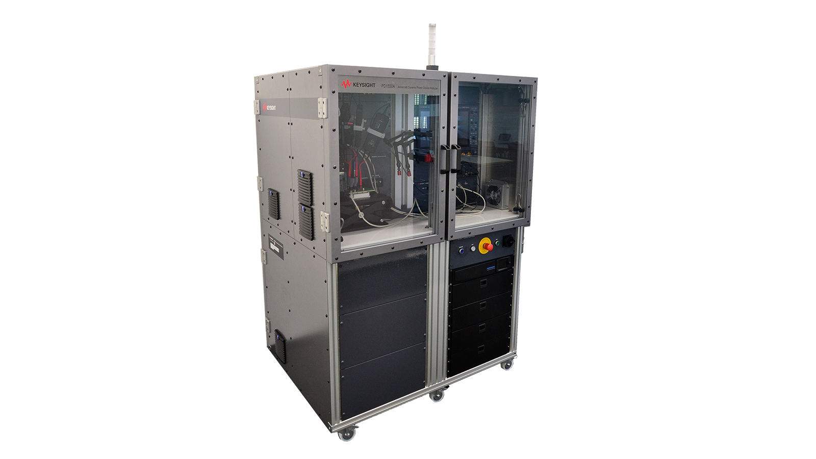
Your safety is critical when testing power semiconductors. Keysight designed multiple safety features into the PD1500A to enhance
your safety. The test environment is covered by a transparent hood, protecting the user from contacting high voltages. When >
42V is energized, the hood is
locked and the red light is illuminated
For further protection, the PD1500A provides an Emergency Off Operation (EMO) button to disconnect
high voltages when pressed
PD1000A Power Device Measurement System for Advanced Modeling
• Easily create models you can trust for any WBG device with real measurements right on your
• Exclusive WBG device modeling results in accurate simulations of EMI, in-rush, overshoots, switching time,
• Easily identify causes of EM noise in simulation, before the design is finalized
• Complete, one-vendor solution of hardware, software, consulting and support services worldwide
Please reference the PD1000A Power Device Measurement System for Advanced Modeling Solution Brochure
( 5992-2700EN ) for more information.
PD1500A Overview and Basic Operation
The PD1500A is designed to be modular, allowing for a variety of devices (SiC, IGBTs, Si MOSFETs and
GaN) and characterization tests (DPT, reverse recovery, gate charge). The system provides complete
DPT characterization and parameter extraction for discrete power semiconductors, supporting maximum
power operation at 1.2 kV and 200 A.
Figure
4. PD1500A block diagram
The PD1500A fixture allows TO-247 (3- or 4-pin) or SMD packages to
interface with the system. Connections for de-skew and AutoCal are
readily available. When high-current and module testing is included,
the system will scale to the appropriate size for the DC-link capacitor
and load inductors. When high performance GaN testing is included,
the gate drivers, clamp circuit, DC–link capacitors and load inductors
条件:SMD; up to 175˚C for TO-247). A small heater is connected directly to the DUT for maximum heat conduction.
The temperature is monitored (K-type thermocouple) and controlled by an internal microcontroller.
The PD1500A enables testing of characteristics over a temperature range (ambient temperature up to 150˚C for
User Configuration, Control and Analysis
条件:available from the local database. A simple semi-automated sequence is shown below.
1. Insert DUTs on the test module
2. Attach heater and thermocouple (if used)
3. Assemble test modules (DUT, clamp, gate driver modules) onto test fixture
4. Connect probes to test modules
5. Set up test parameters in the control software
6. Press "Start"
7. Repeat steps 4 and 5 for reverse recovery diode test or other tests
The PD1500A is controlled with a simple and flexible graphical user interface. It provides test setup,
execution, DPT display and data logging. Both the raw waveform and the extracted parameters are
Figure
6. Example PD1500A user interface
Tested Parameters1,2
Switching locus Id vs Vds3
Reverse recovery current characteristics Id vs. t
Gate Charge4 Total gate charge Qg
Gate charge curve Vgs vs. t
条件:smoothness of the measured curve. High gate resistance (e.g. ≥100 Ohm) is recommended.
Multiple Tests Derived output characteristics Id vs. Vd3
1 Based on IEC
60747 and JESD24 standards
2 Long off time leads to significant loss of inductor current. This leads to limitations of parameter extraction
3 Quality of the characteristics depends on the cleanliness of measured switching characteristics.
4 Gate charge parameter extraction requires gate current monitoring. The quality of gate charge parameters depends on the
Sampling Accuracy 12 ppb +
75 ppb/year
Deskew Accuracy
200 ps (typical)
DC Source Max Voltage
1200 V5
Min Voltage
50 V (standard configuration)
6 V6 (modified configuration)
Min Current
10 A (standard configuration)
100 mA8 (modified configuration)
Voltage Prog. Resolution
23 mV
Measure Voltage Accuracy
2% of range (typical)
Current Accuracy
4% of range (typical)
AC Measure Voltage probe bandwidth
500 MHz
Current shunt bandwidth (compensated)
400 MHz (typical)
Voltage transition time <
10 ns
(depends on DUT response, Rg)
Gate DC Source High / Low Level Voltage (GD1-GD8)
13 V to 29 V / –10 V to 0 V
High / Low Level Voltage (G11-G24)
0 to 28 V / –28 V to 0 V
Voltage Resolution
<0.1 V (typical)
Max Current
10 A (sink and source)
Measure Voltage Accuracy
2% of range (typical)
Current Accuracy
4% of range (typical)
AC Source Timing Resolution / Accuracy
100 ps / 200 ps
Typical 1st Pulse Width
1 to 60 µs
Min Pulse Width (1st Pulse)
1 µs
Max Off-Time between 1st and 2nd Pulse
25 µs9
Min Off-Time between 1st and 2nd Pulse
200 ns10
Max Pulse Width (2nd Pulse)
10 µs11
Min Pulse Width (2nd Pulse)
200 ns8
Measure Voltage probe bandwidth
500 MHz
Current probe bandwidth
800 MHz
5 Capable of characterizing 650 V
1.2 kV, and 1.7 kV- rated devices. Clamp circuit limits max voltage to 400 V.
6 Operation < 50 V is not guaranteed. The minimum voltage can be reduced to 6 V by inserting a
10 kΩ resistor between V+ and V–.
7 Maximum current depends on the drain/collector voltage, load inductance, and on- state resistance of the DUT .
See Figure 9, page
14 for more details.
8 The minimum current can be reduced to 100 mA by using a 100 mΩ shunt resistor. See Figure 9, page
14 for more details.
9 Big values for off -time lead to significant loss of inductor current. This leads to limitations of parameter extraction
10 Smaller values may be possible but are not recommended and tested
11 Second pulse- width must be selected so that max system current is not exceeded
Electrical Modular Components Load Inductors (typical)
120 µH
16.7 µH
DC-Link Capacitor (typical) 800 µF @ ≤
200 V
144 µF @ > 200 V to ≤
400 V
36 µF @ > 400 V to ≤
880 V
TO-247-3, TO-247-4, D2PAK7
Heater (Option H01) Ambient temperature to 175˚C12
System Mechanical Safety Enclosure Size – safety hood closed 92 cm (W) x 72 cm (D) x
151 cm (H)
Size – safety hood open 92 cm (W) x 87 cm (D) x
168 cm (H)
Weight – enclosure only
120.5 kg
Weight – complete system
162.0 kg
SIC Fixture Size 32cm (W) x 25cm (D) x
16cm (H)
Environmental Operating Temperature
20 ˚C to 30 ˚C
Operating Humidity
50 % to 70 % RH, non-condensing
Operating Altitude Up to 2000 m
Storage Temperature
0 to 40 ˚C
Line Power Voltage 200 V to 240 V, ± 10%
50/60 Hz
Protection & Safety Emergency Off switch (EMO)
Oscilloscope protection (Clamp output)
±15 V (typical)
Safety Hood Maximum energy in the system
16 J (typical)
Lock >
42 V13 (typical)
DC-Link capacitor discharged
Over-temperature Shutdown >
50 ˚C (typical)
Interface LAN
10/100/1000 Base-T Ethernet
12 TO -247 only; D2PAK7 limited to 150˚C
13 Safety hood cannot be opened when >
42 V is present in the system
条件:already own a PD1500A system, skip to the PD1500AU section below to order extra accessories.
Figure
9. PD1500 Operating area and internal inductor selection
(Inductor selection: Auto; Second ON pulse-width
200 ns)
How to Order a new PD1500A system14
How to configure your initial order for the PD1500A Dynamic Power Device Analyzer / DPT. If you
PD1500A Core System (1 required)
The core PD1500A system is comprised of all the necessary equipment to perform dynamic / double-
pulse testing. A list is provided below for reference
PD1500A Core System
1 x DPT Oscilloscope with accessories
1 x Oscilloscope protection probe (for more protection probes, order PD1500A-PPR)
1 x
1.2kV high-voltage power supply with accessories
1 x DPT Function generator with accessories
1 x Auto calibration basic pack
1 x DPT Rack & Safety Enclosure with accessories
Fixture Options (1 required)
SIC DPT Fixture for discrete device modular system
条件:Choose the DUT boards that match the device(s) under test. Required to mount the DUT to the fixture.
DUT Boards (1 required)15
SIC DPT Fixture for discrete device modular system
247 DUT Board for discrete TO-247-3 devices
24K DUT Board for discrete TO-247-4 devices
D2P DUT Board for discrete D2PAK7 devices
Coaxial Shunt (1 required)
Choose a coaxial shunt. Required for ID measurements
条件:or equivalent parts for replacement. 15 See Supplemental Characteristics on page 16.
Choose gate driver board pairs (high and low). Required to drive the gates of the high and low devices.
14 PD1500A’s KeysightCare warranty does not cover consumable accessories (Oscilloscope protection probe, DUT boards, Gate
Drivers, Coaxial Shunts, Heater kit, etc.) and non-electrical parts (cables, passive probes, etc.). Please order PD1500AU options
Gate Driver Boards (1 high-side/low-side pair required)16
Choose a coaxial shunt. Required for ID measurements
GD1 Low-side gate drive board, blank Rg
GD2 High-side gate driver boad, blank Rg
GD3 Low-side gate drive board
0 Ohm Rg
GD4 High-side gate driver boad
0 Ohm Rg
GD5 Low-side gate drive board
10 Ohm Rg
GD6 High-side gate driver boad
10 Ohm Rg
GD7 Low-side gate drive board
100 Ohm Rg
GD8 High-side gate driver boad
100 Ohm Rg
G11
±28 V low-side gate driver board, blank Rg
G12
±28 V high-side gate driver board, blank Rg
G13 ±28 V low-side gate driver board
0 Ohm Rg
G14 ±28 V high-side gate driver board
0 Ohm Rg
G15 ±28 V low-side gate driver board
2.5 Ohm Rg
G16 ±28 V high-side gate driver board
252 Ohm Rg
G17 ±28 V low-side gate driver board
4.9 Ohm Rg
G18 ±28 V high-side gate driver board
4.9 Ohm Rg
G19 ±28 V low-side gate driver board
10.1 Ohm Rg
G20 ±28 V high-side gate driver board
10.1 Ohm Rg
G21 ±28 V low-side gate driver board
22 Ohm Rg
G22 ±28 V high-side gate driver board
22 Ohm Rg
G23 ±28 V low-side gate driver board
100 Ohm Rg
G24 ±28 V high-side gate driver board
100 Ohm Rg
条件:design or by type testing. Supplemental characteristics are typical unless otherwise noted.
Supplemental characteristics are not warranted but are descriptions of performance determined either by
条件:Choose at least one clamp circuit board. Required to perform Rds(on) measurements.
System Mechanical DUT Boards Discrete TO-247-3 devices
(Option 247) >
1000 insertion / removal cycles
Discrete TO-247-4 devices
(Option 24K) >
1000 insertion / removal cycles
Gate Driver Boards All Options >
1000 insertion / removal cycles
16 See Supplemental Characteristics on page
16.
Clamp Circuit Board for Rds(on) measurement (1 required)
CB1 Clamp circuit board
DUT Heater Kit (1 required)
Choose at least one heater kit
条件:voltages. Keysight recommends having extra available to ensure uninterrupted test.
H01 DUT Heather Kit for TO-247 and D2PAK
Protection Probe (1 included; extra optional)
The oscilloscope protection probe is a consumable part that protects the oscilloscope from harmful
Software Licenses (PD1020A required)
PD1020A License for Double-Pulse Test Measurement in PD1000A Control Software
条件:If you already own a PD1500A system, use the PD1500AU accessories model number described below.
If you would like to order your first system or a new system, see “How to order a new PD1500A” above.
PD1021A License for Offline Analysis of Double-Pulse Test Measurements
in PD1000A Control Software (requires D9010BSEO)
D9010BSEO Infiniium Offline - Base Software
PD1030A License for GaN Double-Pulse Test Measurements
in PD1000A Control Software (required for Customized GaN)
How to order accessories for an existing system17
PD1500AU – Accessories for the PD1500A18
PD1500AU – Option Description
条件:equivalent parts for replacement. 18 See Supplemental Characteristics on page 16.
please contact your local Keysight office. The complete list is available at:
CB2 Clamp Circuit Board
G01 Low-side gate drive board, blank Rg
G02 High-side gate driver boad, blank Rg
G03 Low-side gate drive board
0 Ohm Rg
G04 High-side gate driver boad
0 Ohm Rg
G05 Low-side gate drive board
10 Ohm Rg
G06 High-side gate driver boad
10 Ohm Rg
G07 Low-side gate drive board
100 Ohm Rg
G08 High-side gate driver boad
100 Ohm Rg
G11
±28 V low-side gate driver board, blank Rg
G12
±28 V high-side gate driver board, blank Rg
G13 ±28 V low-side gate driver board
0 Ohm Rg
G14 ±28 V high-side gate driver board
0 Ohm Rg
G15 ±28 V low-side gate driver board
2.5 Ohm Rg
G16 ±28 V high-side gate driver board
2.5 Ohm Rg
G17 ±28 V low-side gate driver board
4.9 Ohm Rg
G18 ±28 V high-side gate driver board
4.9 Ohm Rg
G19 ±28 V low-side gate driver board
10.1 Ohm Rg
G20 ±28 V high-side gate driver board
10.1 Ohm Rg
G21 ±28 V low-side gate driver board
22 Ohm Rg
G22 ±28 V high-side gate driver board
22 Ohm Rg
G23 ±28 V low-side gate driver board
100 Ohm Rg
G24 ±28 V high-side gate driver board
100 Ohm Rg
17 PD1500A’s KeysightCare warranty does not cover consumable accessories (Oscilloscope protection probe, DUT boards, Gate
Drivers, Coaxial Shunts, Heater kit, etc.) and non-electrical parts (cables, passive probes, etc.). Please order PD1500AU options or
For more information on Keysight Technologies’ products, applications or services,
This information is subject to change without notice. © Keysight Technologies, 2019 - 2024, Published in USA, March 27, 2024
5992-3942EN
PD1500AU – Accessories for the PD1500A (continued)19
PD1500AU – Option Description
H01 DUT Heater Kit for TO-247 and D2PAK
H02 Heater bracket for SIC-Heater
H03 Transistor Isolation Tape
247 DUT Board, TO-247
3-pin
24K DUT Board, TO-247
4-pin
D2P DUT Board, D2PAK
7-pin
19 See Supplemental Characteristics on page
16.
以上指标摘自厂家官方数据手册,完整定义、测试条件与保证值口径以手册为准。完整指标、测试条件与定义口径请见产品页「软件和手册 | 白皮书」栏目中的官方数据手册。
是德科技 | KEYSIGHT · onetest 仪器资源库



 客服








 粤公网安备44030902003758