


 客服




频率范围:9 kHz 至 3/6 GHz
频率转换:5ms
相位噪声(1 GHz,20 kHz 频偏):–119 dBc/Hz
杂散(1 GHz,谐波):–35 dBc
输出功率(1 GHz):+18 dBm
120MHz带宽
ONETEST 欢迎您
厂商登录 | 入驻
登录 | 注册 购物车 微信公众号厂商登录
类似产品
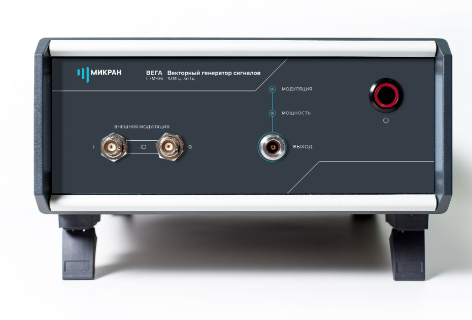
频率范围:10 MHz至6 GHz−90 dBm至+12 dBm的宽输出功率控制范围低相位噪声:−130 dBc/Hz(20 kHz),1 GHz载波偏移模拟调制类型:幅度、频率、相位和脉冲调制自定义数字调制内置调制信号发生器100 MHz 调制信号带宽
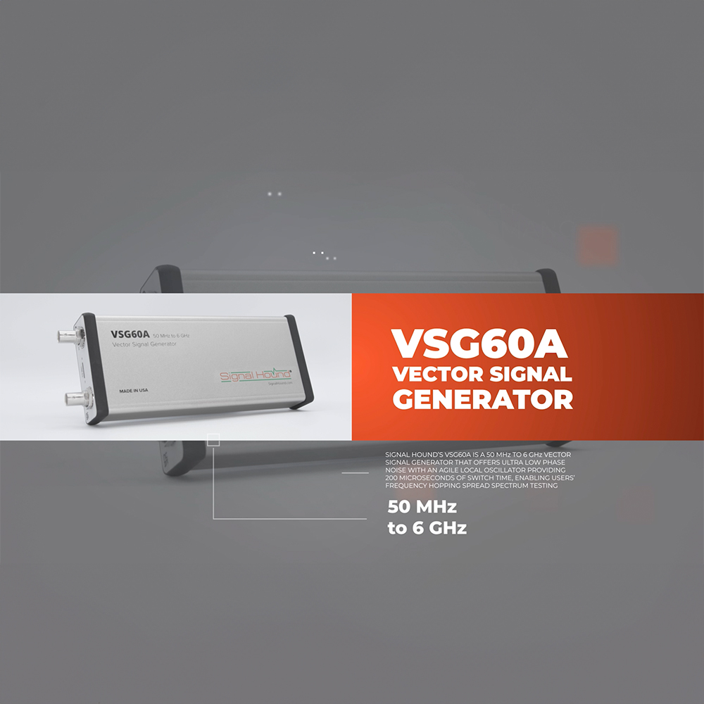
50MHz至6GHz · 40MHz 流式调制带宽 · 200μs 频率切换 · EVM 0.3%
同厂商产品
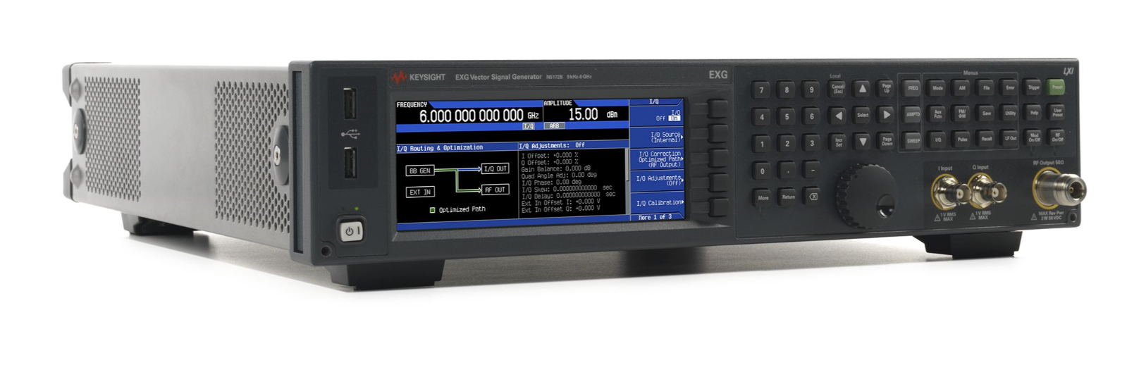
频率范围:9 kHz 至 3/6 GHz频率转换800us相位噪声(1 GHz,20 kHz 频偏):–122dBc/Hz杂散(1 GHz,谐波):–35 dBc输出功率(1 GHz):+21 dBm60/120/160MHz带宽
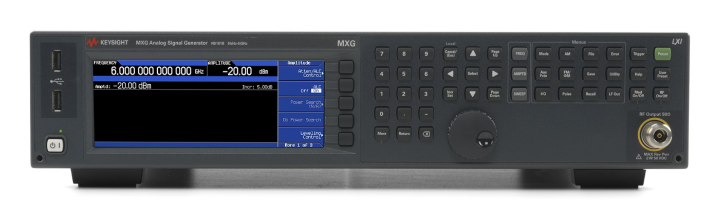
频率范围:9 kHz 至 3/6 GHz频率转换:800 µs相位噪声(1 GHz,20 kHz 频偏):–146 dBc/Hz杂散(1 GHz,谐波):–35 dBc输出功率(1 GHz):+24 dBm
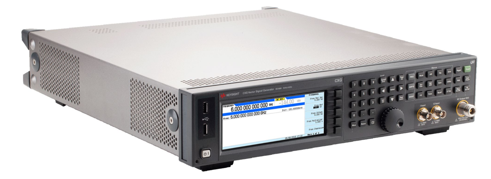
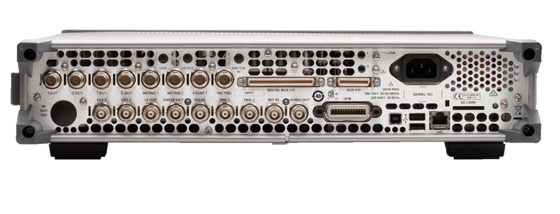
CXG系列N5166B 9 kHz 至 3/6 GHz射频矢量信号发生器 120MHz带宽|是德/KEYSIGHT (在产)
参考价格 : US$ 29,191
产品描述
详细指标
软件和手册|白皮书
购买渠道
选件
问大家
视频
测评
口碑
系统与解决方案
是德科技|KEYSIGHT
XG1 系列矢量信号发生器,6 GHz
矢量信号发生器
产品简介
是德科技N5166B CXG射频矢量信号发生器作为一款专业的射频信号源,提供9kHz至6GHz的频率范围,可帮助您完成各种测试需求。
核心参数
• 1 GHz 谐波:-35 dBc
• 1 GHz 输出功率:18 dBm
• 1 GHz 相位噪声(20 kHz 偏移):-119 dBc/Hz
• 最高频率:6 GHz
• 最大调制带宽:120 MHz
• 输出路数:1
• 频率切换速度:5000 µs
功能特性
• 利用直观且经济高效的信号分析仪进行设计、测试和教学
工程的内涵在于将各种创意有机地结合起来,并解决遇到的问题。
CXA 信号分析仪具有出色的实际性能,是一款卓越且经济高效的基础信号表征工具。
其功能非常强大,为通用用户和教育行业的用户开展测试奠定了坚实的基础。
无论您是希望快速验证成品的质量,还是演示实验教程,它都能帮助您快速获得答案。
利用 9 kHz 至 26.5 GHz 的宽广频率范围,以及高达 25 MHz 的分析带宽,可以观察到更多的信号
为手动和自动制造测试系统增添可靠的信号分析功能
能够执行杂散搜索和失真分析等基本测量
使用可选的内置跟踪发生器,可以进行激励响应测量
结合使用 X 系列测量应用软件,增添更多重要功能
在您的射频和微波教育实验室中使用培训套件,通过实践加深对理论知识的理解
• 专为物联网设备和通用设备的設計与测试而精心打造
覆盖 9 kHz 至 3 或 6 GHz 的频率范围,射频调制带宽高达 120 MHz
可执行基本的元器件参数测试和接收机功能验证
利用多个经过验证且符合标准的矢量信号对您的器件进行测试
利用可靠的矢量信号发生器,轻松对无线通信系统中的元器件进行故障诊断
自主维护解决方案和低成本维修可最大限度地减少停机时间及相关成本
资源下载
以上内容与指标均取自是德科技(KEYSIGHT)官网该产品详情页与官方产品资料,未标注口径的为厂家公布值。
是德科技|KEYSIGHT · onetest 仪器资源库
是德科技 | KEYSIGHT
CXG系列N5166B 9 kHz 至 3/6 GHz射频矢量信号发生器 120MHz带宽 详细指标
矢量信号发生器
一、频率规格
条件:Phase offset Adjustable in nominal 0.1° increments
Frequency range Option 503
9 kHz (5 MHz IQ mode) to 3 GHz
Option 506
9 kHz (5 MHz IQ mode) to 6 GHz
Resolution
0.001 Hz
Frequency bands1 Band Frequency range N
1 9 kHz to < 5 MHz
1 (Digital synthesis)
1 5 to < 250 MHz
1
2 250 to < 375 MHz
0.25
3 375 to < 750 MHz
0.5
4 750 to < 1500 MHz
1
5 1500 to < 3000.001 MHz
2
6 3000.001 to 6000 MHz
4
Frequency switching speed2,3
SCPI, or List/Step sweep mode ≤
5 ms, typical For both CW and digital modulation modes
频率参考
Accuracy ± (time since last adjustment × aging rate) ± temperature
effects ± line 电压 effects ± 校准精度
条件:Temperature effects ±1 ppm (0-55°C), nominal
Line voltage effects ±0.1 ppm, nominal; 5%-10%, nominal
Reference output 10 MHz, > +4 dBm, nominal into 50 Ω load
Internal time base reference oscillator aging rate ≤ ±5 ppm/10 years, <
±1 ppm/year
Initial achievable calibration accuracy ± 4 ×
10-8
Adjustment resolution < 1 ×
10-10
稳定度 Follows 稳定度外部 reference 信号
条件:Amplitude > –3.0 to 20 dBm, nominal
Lock range
±1 ppm
Impedance
50 Ω, nominal
扫描模式 (频率和幅度)
Operating modes Step sweep (equally spaced frequency and amplitude steps)
List 扫描 (arbitrary list 频率和幅度 steps)
Simultaneously sweep waveforms; see Baseband generator section for more detail
扫描范围 Within instrument 频率和幅度量程
Dwell time
100 µs to 100 s
Number of points
2 to 65535 (Step sweep)
1 to 3201 (List sweep)
Step change Linear or logarithmic
条件:1. N is a factor used to help define certain specifications within the document
2. Time from receipt of SCPI command or trigger signal to within 0.1 ppm of final frequency or within 100 Hz, whichever is greater, and amplitude settled to
within 0.2 dB from 20 to 30°C. When switching into or out of band 6, amplitude settling time is within 0.3dB. Implies simultaneous freq and ampl switching.
3. With internal channel corrections on, the frequency switching speed is < 1.3 ms, measured for list mode and SCPI mode cached frequency points. For the
initial frequency point in SCPI mode, the time is < 3.3 ms, measured. The instrument will automatically cache the most recently used 1024 frequencies.
Triggering Free run, trigger key, external, timer, bus (GPIB, LAN, USB)
二、幅度规格
输出参数
条件:1. Quoted specifications between 20 and 30 °C. Maximum output power typically decreases by 0.01 dB/°C for temperatures outside this
Settable range
+19 to -144 dBm
Resolution
0.01 dB
Step attenuator
0 to 130 dB in 5 dB steps, electronic type
Connector Type N
50 Ω nominal
Maximum output level1
9 kHz to 10 MHz
+13 dBm
>10 MHz to 3 GHz
+18 dBm
>3 to 6 GHz
+16 dBm
Absolute level accuracy in CW mode2 (ALC on)
Range Max. power to -60 dBm <
-60 to -110 dBm
9 to 100 kHz ±0.6 dB typical
±0.9 dB typical
100 kHz to 5 MHz ±0.8 dB, ±0.3 dB typical ±0.9 dB
±0.3 dB typical
> 5 MHz to 3 GHz ±0.6 dB, ±0.3 dB typical ±0.8 dB
±0.3 dB typical
>3 to 6 GHz ±0.6 dB, ±0.3 dB typical ±1.1 dB
±0.3 dB typical
Absolute level accuracy in CW mode (ALC off, power search run, relative to ALC on)
9 kHz to 6 GHz
±0.15 dB typical
Absolute level accuracy in digital IQ mode (ALC on, relative to CW, W-CDMA 1 DPCH configuration <
+10 dBm)
5 MHz to 6 GHz ±0.25 dB
±0.05 dB typical
range. 2. Quoted specifications between 20-30°C. For temperature outside this range, absolute level accuracy degrades by 0.01 dB/°C. Output power may drift up to 0.10 dB < 3 GHz and 0.15 dB >
3 GHz per g/kg change in absolute humidity (nom.)
Repeatability measures the ability of the instrument to return to a given
power setting after a random excursion to any other frequency and power
setting. It should not be confused with absolute level accuracy
最大值 reverse 功率, 标称值
< 1 GHz
50 W
> 1 to 2 GHz
25 W
> 2 to 6 GHz
20 W
Max. DC voltage
50 VDC
Trip level
2 W
幅度 switching 速度 CW 模式数字调制模式
SCPI mode ≤ 5 ms, typical ≤
5 ms, typical
Power search SCPI mode < 12 ms, measured <
12 ms, measured
List /Step sweep mode ≤ 5 ms, typical ≤
5 ms, typical
Alternate power level control
Switching time (via waveform marker) 20 µs within
± 1 dB, measured
Functional power range
-15 dBm to -144 dBm, measured
User flatness correction
Number of points
3201
Number of tables Dependent on available free memory in instrument
10,000 maximum
Entry modes USB/LAN direct power meter control, LAN or USB to GPIB, remote bus, and manual
见频率规格 section · more detail
SWR (measured CW mode)
1
频率衰减器 state
条件:1. SWR < 1.60: 1 below 30 kHz
Bypass 0 to 10 dB
15 dB or more
≤ 1.0 GHz < 1.3: 1 < 1.35: 1 < 1.2
1
> 1.0 to 2 GHz < 1.55: 1 < 1.5: 1 < 1.3
1
> 2 to 3 GHz < 1.8: 1 < 1.5: 1 < 1.45
1
> 3 to 4 GHz < 1.5: 1 < 1.6: 1 < 1.7
1
> 4 to 6 GHz < 1.9: 1 < 1.6: 1 < 1.6
1
三、Spectral Purity Specifications
条件:9 kHz to < 5 MHz -65 dBc, nominal
1. Calculated from phase noise performance in CW mode at +10 dBm.
Absolute SSB phase noise CW at 20 kHz offset
5 to 250 MHz
-116 dBc/Hz, typical
250 MHz
-130 dBc/Hz, typical
500 MHz
-125 dBc/Hz, typical
1 GHz
-119 dBc/Hz, typical
2 GHz
-112 dBc/Hz, typical
3 GHz
-107 dBc/Hz, typical
4 GHz
-106 dBc/Hz, typical
5 GHz
-105 dBc/Hz, typical
6 GHz
-103 dBc/Hz, typical
Residual FM (CW mode
300 Hz to 3 kHz BW, CCITT, rms
5 MHz to 6 GHz < N ×
2 Hz (measured); See N value in frequency band table
Residual AM (CW mode, 0.3 to 3 kHz BW, rms
+5 dBm
100 kHz to 3 GHz <
0.01% (measured)
Harmonics (CW mode) Input power <
+4 dBm
9 kHz to 3 GHz <
-35 dBc
> 3 to 4 GHz <
-35 dBc, typical
> 4 to 6 GHz <
-53 dBc, typical
Non-harmonics (CW mode) >
10 kHz offset
5 to <250 MHz
-75 dBc
250 to < 750 MHz
-75 dBc
750 MHz to < 1.5 GHz
-72 dBc
1.5 to <3.0 GHz
-66 dBc
3 to 6 GHz
-60 dBc
Sub-harmonics (CW mode)
9 kHz to 1.5 GHz None
> 1.5 to 3 GHz
-77 dBc
> 3 to 6 GHz
-74 dBc
Jitter1
Carrier frequency SONET/SDH data rate rms jitter BW µUI rms Seconds
155 MHz 155 MB/s 100 Hz –1.5 MHz 140 (meas.)
0.9 ps typical
622 MHz 622 MS/s 1 kHz – 5 MHz 67
0.11 ps
2.488 GHz 2488 MB/s 5 kHz – 20 MHz 271
0.11 ps
四、Analog 调制规格
条件:Max. deviation N × 10 MHz, nominal
Resolution 0.025% of deviation or 1 Hz, whichever is greater, nominal
Modulation frequency response @100 kHz rate 1 dB bandwidth DC/5 Hz to 3 MHz, nominal
3 dB bandwidth DC/1 Hz to 7 MHz, nominal
FM using external input 1 or 2 Sensitivity +1V peak for indicated deviation, nominal
Input impedance 50Ω/600Ω/1MΩ, nominal
Frequency modulation (Option UNT) (See N value in Frequency Specification section)
Deviation accuracy < ±2% + 20 Hz (1 kHz rate, deviation is N ×
50 kHz)
Carrier frequency accuracy < ±0.2% of set deviation + (N × 1 Hz)
1
Relative to CW in DCFM < ±0.06% of set deviation + (N ×
1 Hz)2, typical
Distortion < 0.4% [1 kHz rate, deviation is N ×
50 kHz]
Paths FM path 1and
2 are summed internally
for composite modulation
条件:Maximum deviation3 Normal bandwidth N × 5 radians, nominal
High-bandwidth mode N × 0.5 radians, nominal
Frequency response Normal bandwidth (3 dB) DC to 1 MHz, nominal
High-bandwidth mode (3 dB) DC to 4 MHz, nominal
ΦM using external input 1 or 2 Sensitivity +1V peak for indicated deviation, nominal
Input impedance 50Ω/600Ω/1MΩ, nominal
Phase modulation (Option UNT) (See N value in Frequency Specification section)
Resolution
0.1% of deviation
Deviation accuracy <
+0.5%+0.01 rad, typical [1 kHz rate, normal bandwidth mode]
Distortion <
0.2% typical [1 kHz rate, normal bandwidth mode]
Paths ΦM path 1and
2 are summed internally
for composite modulation 1. Specification valid for temperature changes of less than ±5°C, since last DCFM calibration 2. Typical performance immediately after a DCFM calibration 3. Digital synthesis band FM deviation is
5 MHz
AM depth type Linear or exponential
条件:Depth resolution 0.1% of depth, nominal
Frequency response wideband AM Rates ALC Off/On DC/800 Hz to 80 MHz, nominal
Maximum depth
100%
AM depth error @ 1kHz rate and <
80%
depth F < 5 MHz <1.5% of setting + 1% (typ. 0.5% of setting +
1%)
5 MHz ≤ F ≤ 2 GHz <3% of setting +
1 %
2 < F ≤ 3 GHz <5% of setting + 1% (typ. 3% of setting +
1%)
3 < F ≤ 6 GHz (typical 4% of setting +
1%)
Total harmonic distortion @
1 kHz rate at 30% depth at 80% depth
F < 5 MHz <0.25%, typical <
0.5%, typical
5 MHz ≤ F < 2 GHz < 2% <
2%
2 ≤ F < 3 GHz < 2%, typical <
2%, typical
Frequency response 30% depth
3 dB BW DC/10 Hz to 50 kHz
AM inputs using external inputs
1
or 2
Sensitivity 1 Vpeak for indicated depth (Over-range can be
200% or 2.2
Input impedance 50 Ω or 600 Ω or 1 MΩ; Damage level
±5 Vmax
Path AM path 1 and path
2 are summed internally for
composite modulation
条件:Input impedance 50 Ω, nominal, Input via I only
Wideband AM inputs Sensitivity
1 V peak-to-peak sine wave signal with 0.5V DC offset
required input for 100% AM
Simultaneous modulation
All modulation types (I/Q, AM, FM, ΦM and pulse modulation) may be simultaneously enabled, except: FM and ΦM cannot be
combined and two modulation types cannot be simultaneously generated using the same modulation source. For example, the
baseband I/Q generator, AM and FM can run co-currently and all will modulate the output RF (this is useful for simulating
Composite modulation
AM, FM, and ΦM each consist of two modulation paths which are summed internally for composite modulation; modulation
“+” = compatible, “-” = incompatible
条件:Frequency accuracy Same as RF reference source, nominal
LF audio output 0 to 5 Vpeak into 50 Ω, -5V to 5V offset, nominal
External modulation inputs (Option UNT required for AM, FM, ΦM modulation input; Option UNW required for pulse modulation inputs)
EXT
1 AM, FM, ΦM
EXT
2 AM, FM, ΦM
PULSE Pulse (50 Ω only)
I Wideband AM (50 Ω only)
Input impedance 50 Ω, 1 MΩ
600 Ω, DC and AC coupled
Standard internal analog modulation source (Single sine wave generator for use with AM, FM, ΦM; Requires Option UNT or 303)
Waveform Sine, Square, Triangle, Positive ramp, Negative ramp
Rate range
0.1 Hz to 2 MHz (tunable to 3 MHz)
Resolution
0.1 Hz
Multifunction generator (Option
303)
The multifunction generator option (Option 303) consists of seven waveform generators that can be set independently with
up to five simultaneously using the composite modulation features in AM, FM/PM, and LF out
条件:DC Only for LF output -5V to +5V, nominal
Function generator
1 Sine, Triangle, Square, Positive ramp, Negative ramp, Pulse
Function generator
2 Sine, Triangle, Square, Positive ramp, Negative ramp, Pulse
Dual function generator Sine, Triangle, Square, Positive ramp, Negative ramp, Phase offset and
amplitude ratio for Tone 2 relative to Tone
1
Swept function generator Sine, Triangle, Square, Positive ramp, Negative ramp
Trigger: free run, trigger key, bus, external, internal, timer trigger
Noise generator
1 and 2 Uniform, Gaussian
条件:Sine wave 0.1 Hz to 10 MHz, nominal
Triangle, Square, Ramp, Pulse 0.1 Hz to 1 MHz, nominal
Noise bandwidth 10 MHz, nominal
Frequency accuracy Same as RF reference source, nominal
Width compression (RF width relative to video out) < 5 ns, typical 1. Pulse specifications apply to frequencies > 100 MHz and power set to > -3 dBm. Operable down to 9 kHz 2. With power search on
Resolution
0.1 Hz
Narrow pulse modulation (Option UNW)
1
On/Off ratio >
80 dB, typical
Rise/Fall times (Tr, Tf) < 10 ns
7 ns typical
Minimum pulse width ALC on/off ≥ 2µs / ≥
20ns
Repetition frequency ALC on/off
10 Hz to 500 kHz / DC to 10 MHz
Level accuracy relative to CW ALC on/off2 < ± 1.0 dB, ± 0.5 dB typical / <
± 0.5 dB typical
Narrow pulse modulation (continued)
条件:External video delay (ext. input to video) 30 ns, nominal
RF delay (video to RF output) 20 ns, nominal
Input level +1 V peak = RF on into 50 Ω, nominal
Video feed-through1, ≤
3 GHz / >
3 GHz < 50 mV typical / <
5 mV typical
Pulse overshoot
<15%, typical
Internal pulse train generator (included in option UNW)
条件:Square wave rate 0.1 Hz to 10 MHz, 0.1 Hz resolution, nominal
Pulse period 30 ns to 42 seconds, nominal
Mode Free-run, Square, Triggered, Adjustable doublet, Trigger doublet, Gated, External Pulse
Pulse width
条件:Resolution 20 ns to pulse period –10 ns, nominal 10 ns
Resolution (delay, width, period) 10 ns nominal
1. Video feedthrough applies to power levels < +10 dBm
Adjustable trigger delay (-pulse period +
10 ns) to (pulse width – 10 ns)
Settable delay Free run
-3.99 to 3.97 µs
Triggered
0 to 40 s
Pulse doublets 1st pulse delay (relative to sync out)
0-42s – pulse width – 10 ns
1st pulse width
500 ns to 42 s – delay – 10 ns
2nd pulse delay 0 to 42 s – (Delay 1 + width
2) – 10 ns
2nd pulse width 20 ns to 42 s – (Delay 1+ Delay
2) – 10 ns
Pulse train generator (N5180320B)
Number of pulse patterns
2047
On/Off time range
20 ns to 42 sec
五、矢量调制规格
条件:Bandwidth Baseband (I or Q) Up to 100 MHz, nominal
RF (I + Q) Up to 200 MHz, nominal
Full scale input drive (I + Q) 0.5V into 50Ω, nominal
Impedance 50 Ω, nominal per output
IQ modulator external inputs
1
I or Q offset
±100 mV (200 µV resolution)
I/Q gain balance
± 4 dB (0.001 dB resolution)
I/Q attenuation
0 – 50 dB (0.01 dB resolution)
Quadrature angle adjustment
± 200 units
Internal I/Q baseband generator adjustment (option
653 and 655)
I/Q offset
± 20% (0.025% dB resolution)
I/Q gain
± 1 dB (0.001 dB resolution)
Quadrature angle adjustment
± 10° (0.01 degrees resolution)
I/Q phase
± 360.0° (0.01 degrees resolution)
I/Q skew
± 500 ns (1 ps resolution)
I/Q delay
± 250 ns (1 ps resolution)
Internal IQ outputs
1
Type Single-ended
条件:Bandwidth (I, Q) Baseband (I or Q) 60 MHz, nominal (opt.653, 655)
RF (I+Q) 120 MHz, nominal (opt. 653, 655)
Amplitude flatness ± 0.2dB, measured with channel corrections optimized for I/Q output
Phase flatness ± 2.5 degrees measured with channel corrections optimized for I/Q output
1. I/Q adjustments represent user interface nominal parameter ranges and not specifications
2. Intern I/Q adjustments apply to RF out and I/Q outputs simultaneously
Internal real time complex digital I/Q filters (included with option 653)
Maximum voltage per output 1V peak-to-peak, or 0.5Vpeak Into
50 Ω (200µV resolution)
Common mode I/Q offset ±1.5V into
50Ω (200 µV resolution)
Factory channel correction (256 taps)
Corrects the linear phase and amplitude response of the baseband I/Q and RF outputs of the signal generator, using
factory calibration arrays (default mode is off)
RF amplitude flatness (120 MHz)
±0.2 dB measured
RF phase flatness (120 MHz)
±2 degrees measured
User channel correction (256 taps)
Automated routine uses USB power sensor to correct for linear phase and amplitude response of DUT. See User’s Guide
for more detail
条件:RF bandwidth (I+Q) Option 653 60 MHz, nominal
Option 653 and 655 120 MHz, nominal
Max. RF amplitude flatness correction
±15 dB
Max. RF phase flatness correction
± 20 degrees
Equalization filter (256 taps)
User can download and apply inverse or custom phase and amplitude response coefficients from tools such as MATLAB,
89601B VSA, or SystemVue to correct for linear errors of DUT/system. See User’s Guide for more detail
Baseband generator (Option 653
655)
Channels
2 (I and Q)
Resolution
12 bits
Sample rate Option 653
100 Sa/s to 75 MSa/s
Option 653 and 655
100 Sa/s to 150 MSa/s
Interpolated DAC rate 800 MHz (waveforms only need OSR=
1.25)
Frequency offset range
±80 MHz
Digital sweep modes In list sweep mode, each point in the list can have independent waveforms along with user
definable frequencies and amplitudes; See Frequency Specifications section for more detail
Waveform switching speed1 ≤
5 ms, measured, in both SCPI mode and List/Step sweep mode
Waveform transfer rates (Measured, no markers, unencrypted)
条件:1. SCPI mode switching speed applies when waveforms are pre-loaded in list sweep and sample rate ≥ 10 MSa/s.
FTP LAN to internal SSD
10.7 MB/sec or 2.67 MSa/sec
Internal SSD to FTP LAN 7.7 MB/sec
1.92 MSa/sec
FTP LAN to BBG
8.2 MB/sec or 2.05 MSa/sec
FTP LAN to BBG encrypted
4 MB/sec or 1 MSa/sec
USB to BBG
19 MB/sec or 4.75 MSa/sec
BBG to USB
1.2 MB/sec or 300 kSa/sec
Internal SSD to BBG
48 MB/sec or 12 MSa/sec
BBG to internal SSD
1.2 MB/sec or 300 kSa/sec
Arbitrary waveform memory Max. playback capacity 32 MSa standard, 512 MSa with Opt.
022
Max. storage capacity incl. markers 3 GB/800 MSa
30GB/7.5GSa with opt.009
Waveform segments Segment length
60 samples to 32 MSa, standard
60 samples to 512 MSa, requires opt.022
Min. memory allocation per segment
256 samples
Max. number of segments
8192
Waveform sequences Max. number of sequences >
2000 depending on non-volatile memory usage
Max. number of segments/sequence 32,000 (standard), 4 million (opt.
022)
Max. number of repetitions
65,535
Segment advance Single or continuous
条件:Trigger latency (single trigger only) 356 ns + 1 sample clock period, nominal
Trigger accuracy (single trigger only) ± 2.5 ns, nominal
Trigger repeatability < 1 ns, nominal
External coarse delay time
5 ns to 40 s
External coarse delay resolution
5 ns
Single trigger – restart on trigger mode will initiate a FIFO clear.
Multi-baseband generator synchronization mode (multiple sources)
Fan out
1 primary and up to 15 secondary
See Internal I/Q Baseband section
Markers Markers are defined in a segment during the waveform generation process, or from the front
panel; a marker can also be routed to the RF blanking, ALC hold functions, and alternate
Marker polarity Negative, positive
Number of markers
4
RF blanking/Burst On/Off ratio >
80 dB
Nyquist, root-Nyquist, WCDMA, EDGE,
Gaussian, rectangular, APCO
25 C4FM, IS-95
User FIR
条件:Applies real-time FIR filtering when playing waveforms with OSR=1. Helps to reduce waveform size for long simulation times.
Bandwidth With option 653 1 Hz to 60 MHz
With option 653 and 655 1 Hz to 120 MHz
Option
660 not required
AWGN (N5180403B)
Type Real-time, continuously calculated, and played using DSP
Modes of operation Standalone, or digitally added to signal played by arbitrary waveform
Crest factor
15 dB
Randomness 90 bit pseudo-random generation, repetition period 313 ×
109 years
Carrier-to-noise ratio
± 100 dB when added to signal
Carrier-to-noise formats C/N, Eb/No
Carrier-to-noise ratio error Magnitude error ≤
0.2 dB at baseband I/Q input
Custom modulation ARB mode (N5180431B)
Modulation PSK BPSK, QPSK, OQPSK, π/4DQPSK, gray coded and
unbalanced QPSK, 8PSK
16PSK, D8PSK
QAM 4, 16, 32, 64, 128, 256, 1024 (and
89601B VSA mappings)
FSK Selectable: 2, 4, 8
16, C4FM
MSK
0 to 100°
ASK
0 to 100%
Multicarrier Number of carriers Up to 100 (limited by a max BW of 120 MHz depending on
symbol 速率和调制类型)
Frequency offset (per carrier) Up to -60 to +60 MHz
Power offset (per carrier)
0 to -40 dB
Symbol rate
50 sps to 100 Msps
Filter types Nyquist, root-Nyquist, Gaussian, rectangular, APCO
25 C4FM, user
Quick setup modes APCO
25w/C4FM, APCO25 w/CQPSK, Bluetooth®, CDPD, DECT, EDGE, GSM, NADC, PDC, PHS
Data Random only
Custom modulation real-time mode (N5180431B) (Does not require option
660)
Modulation PSK BPSK, QPSK, OQPSK, π/4DQPSK, gray coded and
unbalanced QPSK, 8PSK
16PSK, D8PSK
QAM 4, 16, 32, 64, 128, 256, 1024 (and
89601B VSA mappings)
FSK Selectable: 2, 4, 8
16, C4FM
Custom map of up to 16 deviation levels
Max. deviation
20 MHz
MSK
0 to 100°
ASK
0 to 100%
DVB-S2 APSK 16APSK 2/3, 16APSK 3/4, 16APSK 4/5, 16APSK 5/6, 16APSK
8/9
16APSK 9/10, 32APSK 3/4, 32APSK 4/5, 32APSK 5/6, 32APSK
8/9
32APSK
9/10
Custom I/Q Custom map of 1024 unique values
Frequency offset Up to -60 to +60 MHz
Symbol rate Internal generated data 1 sps to 100 Msps of max. of 10 bits per symbol (option
653+655)
External serial data
1 sps to [(50 Mbits/sec) / (# bits/symbol)]
Filter types Selectable Nyquist, root-Nyquist, Gaussian, rectangular, APCO 25 (phase
1
and 2 UL and DL), IS-95, WCDMA, EDGE (wide and HSR)
IS-95 w/EQ, IS-95 Mod, IS-95 Mod w/EQ, HDQPSK, APCO25
Custom 调制 real-时间模式 (continued)
Filter type Custom FIR
16-bit resolution, up to 64 symbols long, automatically resampled to 1024
coefficients (max)
> 32 to 64 symbol filter: symbol rate ≤
12.5 MHz
> 16 to 32 symbol filter: symbol rate ≤
25 MHz
Internal filters switch to 16 tap when symbol rate is between
25 and 100 MHz
Quick setup modes APCO 25 with (C4FM, CQPSK, HCPM, HDQPSK), TETRA , Bluetooth, CDPD, DECT, EDGE, GSM, NADC
PDC, PHS, PWT, WorldSpace, Iridium, ICO, CT2, TFTS
16APSK 2/3, 16APSK 3/4, 16APSK 4/5, 16APSK 5/6, 16APSK 8/9, 16APSK 9/10, 32APSK 3/4, 32APSK
4/5
32APSK 5/6, 32APSK 8/9, 32APSK
9/10, SOQPSK
Trigger delay Range
0 to 1,048,575 bits
Resolution
1 bit
Data type Internal generated Pseudo-random patterns PN9, PN11, PN15, PN20, PN23
Repeating sequence Any
4-bit sequence
Direct-pattern RAM max. size (Used for custom TDMA or non-standard framing) 32 Mb (standard) 1024 Mb (option
022)
User filer
32 Mb (standard)
1024 Mb (option
022)
输入/输出 Data, symbol sync, bit 时钟
条件:Frequency spacing 100 Hz to 120 MHz (with option 653, 655)
Phase (per tone) Fixed or random 1. ACPR specifications apply when the instrument is maintained within ± 20 to 30 °C. 2. This is rms power. Convert from rms to peak envelope power (PEP) with the following equation: PEP = rms power + crest factor (for example, 3GPP test model 1 with 64 DPCH has a crest factor 11.5 dB, therefore at +5 dBm rms, the PEP = 5 dBm + 11.5 dB = +16.5
1. ACPR specifications apply when the instrument is maintained within ± 20 to 30 °C.
2. This is rms power. Convert from rms to peak envelope power with the following equation: PEP = rms power + crest factor (for
3. ACPR measurement configuration: reference channel integration BW: 9.015 MHz, offset channel integration bandwidth: 9.015 MHz.
Internal burst shape Rise/Fall time range Up to 30 bits
(varies with bit rate) Rise/Fall delay range
-15 to +15 bits
Multitone and two-tone (requires N5180430B)
Number of tones
2 to 512, with selectable on/off state per tone
dBm PEP). 3GPP W-CDMA distortion performance
2
Offset Configuration Frequency Power level ≤
2 dBm3
Adjacent (5 MHz) 1 DPCH, 1 carrier 1800 to 2200 MHz -69 dBc
-73 dBc typical
Alternate (10 MHz) -70 dBc
-75 dBc typical
Adjacent (5 MHz) Test model
1 with
64 DPCH
1 carrier
1800 to 2200 MHz -68 dBc
-70 dBc typical
Alternate (10 MHz) -68 dBc
-73 dBc typical
Adjacent (5 MHz) Test model
1 with
64 DPCH
4 carrier
1800 to 2200 MHz -63 dBc
-65 dBc typical
Alternate (10 MHz) -64 dBc
-66 dBc typical
example, 3GPP test model 1 with 64 DPCH has a crest factor
11.5 dB, therefore at +5 dBm rms
the PEP = 5 dBm + 11.5 dB =
+16.5 dBm PEP).
3GPP LTE-FDD distortion performance1
Offset Configuration Frequency Power level ≤ 2 dBm
2
Adjacent (10 MHz) 3 10 MHz E-TM
1.1 QPSK
1800 to 2200 MHz -64 dBc
-66 dBc typical
Alternate (20 MHz) 3 -66 dBc
-68 dBc typical
GSM/EDGE output RF spectrum (ORPS) GSM EDGE
Offset Configuration Frequency Power level < +7 dBm Power level <
+7
dBm 200 kHz 1 normal timeslot, bursted
800 to 900 MHz
1800 to 1900 MHz
-34 dBc
-37 dBc
400 kHz -69 dBc
-69 dBc
600 kHz -81 dBc
-80 dBc
800 kHz -82 dBc
-82 dBc
1200 kHz -84 dBc
-83 dBc
3GPP2 cdma2000 distortion performance
Offset Configuration Frequency Power level ≤ +2 dBm
2
885 kHz to 1.98 MHz
9 channel forward
link
800 to 900 MHz
-78 dBc
> 1.98 to 4.0 MHz
-86 dBc
> 4.0 to 10 MHz
-91 dBc
EVM performance
2
Format GSM EDGE cdma2000/IS95 W-CDMA LTE-FDD3
Modulation type GMSK (bursted) 3pi/8 8PSK (bursted) QPSK QPSK
64 QAM
Modulation rate 270.833 ksps 70.833 ksps 1.2288 Mcps 3.84 Mcps
10 MHz BW
Channel config. 1 timeslot 1 timeslot Pilot channel 1 DPCH E-TM
3.1
Frequency
4
800 to 900 MHz
1800 to 1900 MHz
800 to 900 MHz
1800 to 1900 MHz
800 to 900 MHz
1800 to
1900 MHz
1800 to
2200 MHz
1800 to
2200 MHz
EVM power level ≤ 7 dBm ≤ 7 dBm ≤ 7 dBm ≤ 7 dBm ≤
7 dBm
EVM/global phase error 0.2° typical 0.75° typical 0.8° typical 0.8° typical
0.2° typical
EVM performance
条件:1. EVM specifications apply for the default ARB file setup conditions with the default ARB files supplied with the instrument.
2. EVM specifications apply after execution of I/Q calibration when the instrument is maintained within ± 5 °C of the
calibration temperature. 3. LTE FDD E-TM 3.1,10 MHz, 64 QAM PDSCH, full resource block. Measured EVM after DC calibration. 4. Performance evaluated at bottom, middle, and top of bands shown. 5. WLAN 802.11ac 80 MHz, 256 QAM, MCS 8, 7 symbols, no filtering. Channel corrections enabled. Rx equalizer training:
Format 802.11a/g 802.11ac 5 QPSK
16 QAM
Modulation type 64 QAM
256 QAM QPSK QPSK
Modulation rate 54 Mbps 80 MHz BW 4 Msps (root-Nyquist filter ą =
0.25)
Frequency
4
2400 to 2484 MHz ≤ 3 GHz ≤ 6 GHz ≤ 3 GHz ≤
6 GHz
5150 to 5825 MHz
5775 MHz
EVM power level ≤ -5 dBm ≤ -5 dBm ≤ 4 dBm ≤ 4 dBm ≤ 4 dBm ≤
4 dBm
EVM 0.3% measured 0.4% measured 0.8% typical 1.1% typical 0.65% typical
0.9% typical
六、通用规格
温度范围
Operating
0 to 55 °C
Storage
-40 to 70 °C
工作和存储海拔
Up to 15,000 feet
Complies with European EMC Directive
2004/108/EC:
̶ IEC/EN
61326-2-1
̶ CISPR 11, Group
1, Class A
̶ AS/NZS CISPR
11
̶ ICES/NMB-001
This ISM device complies with Canadian ICES-001
Cet appareil ISM est conforme à la norme NMB-001 du Canada
Complies with European Low Voltage Directive
2006/95/EC
–– IEC/EN
61010-1
–– Canada: CSA C22.2 No.
61010-01
–– USA: UL 61010-1
2nd edition
Acoustic noise emission Geraeuschemission
LpA < 70 dB LpA <
70 dB
Normal position Normaler Betrieb
Per ISO 7779 Nach DIN
45635 t.19
Environmental stress
条件:limited to temperature, humidity, shock, vibration, altitude and power line conditions. Test Methods are aligned with IEC
Samples of this product have been type tested in accordance with the Keysight Environmental Test Manual and verified to
be robust against the environmental stresses of Storage, Transportation and End-use; those stresses include but are not
60068-2 and levels are similar to MIL-PRF-28800F Class
3.
供电要求
条件:Voltage and frequency (nominal) 100/120 V, 50/60/400 Hz The instruments can operate with mains supply
voltage fluctuations up to ± 10% of the nominal
1. From 40°C to 55°C, the maximum % Relative Humidity follows the line of constant dew point
voltage 220/240 V
50/60 Hz
Power consumption
300 W maximum
远程编程
Interfaces GPIB IEEE-488.2
1987 with listen and talk
LAN
1000BaseT LAN interface, LXI Class C compliant
USB Version
2.0
Control languages SCPI Version
1997.0
Compatibility languages
Keysight Technologies: N5181A\61A, N
5182A\62A, N5183A, E4438C, E4428C
适用型号 E442xB, E443xB, E8241A, E8244A, E8251A, E8254A, E8247C, E8257C/D,
E8267C/D, 8648 Series, 8656B, E8663B, 8657A/B, 8662A
8663A
Aeroflex Inc.
3410 Series
数据存储
条件:Internal 3 GB (30 GB with option 009)
External Supports USB
2.0 compatible memory devices
Height
88 mm (3.5 in)
Width
426 mm (16.8 in)
Length
489 mm (19.2 in)
校准周期
The recommended calibration cycle is 3 year; calibration services are available through Keysight service centers
前面板面板连接器
RF output Outputs the RF signal via a precision N type female connector; see output section for reverse
I 和 Q 输入
条件:BNC input accepts “in-phase” and “quadrature” input signals for I/Q modulation; nominal input
impedance is 50 Ω, damage levels are
1 Vrms and 5 Vpeak
USB
2.0
Used with a memory stick for transferring instrument states, licenses and other files into or out
of the instrument; also used with U2000, U848X, and U202X Series USB power sensors
后面板面板连接器
Rear panel inputs and outputs are 3.3 V CMOS, unless indicated otherwise; CMOS inputs will accept 5 V CMOS
3 V CMOS, or TTL
电压电平
条件:I and Q outputs BNC outputs the analog I/Q modulation signals from the internal baseband generator; nominal
output impedance 50 Ω, DC coupled; damage levels
± 2 V
Event
1
This connector outputs the programmable timing signal generated by marker
1
The marker signal can also be routed internally to control the RF blanking and ALC hold
functions; this signal is also available on the AUX I/O connector
Pattern trigger Accepts signal to trigger internal pattern generator to start single pattern output, for use with the
internal baseband generators
Accepts CMOS signal with minimum pulse width of 10 ns
Female BNC
条件:EXT 1 External AM/FM/PM #1 input; nominal input impedance is 50 Ω/600 Ω/1M Ω, nominal; damage
EXT 2 External AM/FM/PM #1 input; nominal input impedance is 50 Ω/600 Ω/1M Ω, nominal; damage
LF out 0 to 5 V peak into 50 Ω, –5 V to 5 V offset, nominal
Damage levels are > +8 V and <
–4 V
BBTRIG 1 For arbitrary and real-time baseband generators I/O such as Markers or trigger inputs
BBTRIG 2 For arbitrary and real-time baseband generators I/O such as Markers or trigger inputs
Sweep out Generates output voltage
0 to +10 V when the signal generator is sweeping; this output can
also be programmed to indicate when the source is settled or output pulse video and is TTL
and CMOS compatible in this mode; output impedance < 1 Ω, can drive
2 kΩ; damage levels
are
± 15 V
levels are
± 5 V
levels are
± 5 V
条件:V and high logic levels are +1 V; nominal input impedance is 50 Ω; input damage levels are ≤ –
External pulse modulation input; this input is TTL and CMOS compatible; low logic levels are
0
0.3 V and ≥
+5.3 V
Trigger in
Accepts TTL and CMOS level signals for triggering point-to-point in sweep mode; damage
levels are ≤ –0.3 V and ≥
+5.3 V
Trigger out
Outputs a TTL and CMOS compatible level signal for use with sweep mode
The signal is high at start of dwell, or when waiting for point trigger in manual sweep mode, and
低 when 驻留 over 或 point 触发 received
This output can also be programmed to indicate when the source is settled, pulse
synchronization, or pulse video
Nominal output impedance
50 Ω
Input damage levels are ≤ –0.3 V and ≥
+5.3 V
后面板面板 (continued)
条件:nominal input level –3 to +20 dBm, impedance 50 Ω, sine or square waveform
+3.9 dBm; nominal output impedance 50 Ω; input damage level is +16 dBm
Reference input Accepts a
10 MHz reference signal used to frequency lock the internal timebase
Option
1ER adds the capability to lock to a frequency from 1 MHz to 50 MHz
10 MHz reference out Outputs the
10 MHz reference signal used by internal timebase; level nominally
Reserved for future use
USB 2.0 The USB connector provides remote programming functions via SCPI
GPIB interface The GPIB connector provides remote programming functionality via SCPI
LAN TCP/IP interface The LAN connector provides the same SCPI remote programming functionality as
the GPIB connector and is also used to access the internal Web server and FTP
Supports DHCP, sockets SCPI, VXI-11 SCPI, connection moni
以上指标摘自厂家官方数据手册,完整定义、测试条件与保证值口径以手册为准。完整指标、测试条件与定义口径请见产品页「软件和手册 | 白皮书」栏目中的官方数据手册。
是德科技 | KEYSIGHT · onetest 仪器资源库
全部
是德科技官方渠道
官方渠道(官网 / 热线 / 邮箱)
• 销售服务热线
800-810-0189(座机)/400-810-0189(手机) 工作时间 周一至周五 8:30-17:30
• 热线传真
800-820-2816(座机)/400-820-3863(手机)
• 亚洲区支持邮箱 tm_asia@keysight.com
• 服务与支持邮箱
instruments_services@keysight.com
• 官网
www.keysight.com(中国站 www.keysight.com.cn)
全国办事处
• 北京总部
是德科技(中国)有限公司 北京市朝阳区望京北路3号
电话:(010) 64397888
传真:(010) 64390278
邮编:100102
• 上海分公司
上海市虹口区四川北路1350号中信泰富申虹广场5楼、16-19楼
电话:(021) 36127688
传真:(021) 36127188
邮编:200080
• 广州分公司
广州市天河北路233号中信广场66层07-08室
电话:(020) 38113988
传真:(020) 86695074
邮编:510613
• 深圳分公司
深圳市福田中心区福华一路六号免税商务大厦3楼
电话:(0755) 83079588
传真:(0755) 82763181
邮编:518048
• 成都分公司
成都高新区南部园区天府四街116号
电话:(028) 83108888
传真:(028) 85330830
邮编:610041
• 西安分公司
西安市碑林区南关正街88号长安国际大厦D座5/F
电话:(029) 88867770
传真:(029) 88861330
邮编:710068
• 中国香港
是德科技香港有限公司 中国香港北角电气道169号25楼
电话:(852) 31977777
传真:(852) 25069292 香港热线 800-938-693
• 维修 / 校准服务中心
中国大陆 北京 / 成都 / 苏州 服务热线 800-810-0189 / 400-810-0189
授权分销商
• 上海信果电子科技有限公司(上海)
上海市沪闵路8075号虹梅商务大厦6楼609室
邮编:200233
电话:021-64518399
传真:021-54560890
邮箱:jason.wu@signalgroup.com.tw
• 上海精测电子有限公司(上海)
上海市北京东路668号西楼15E
邮编:200001
电话:13916371522
传真:021-53086102
邮箱:yangzhen@jingce.com
• 北京东方中科集成科技股份有限公司(北京)
北京市海淀区复兴路69号院12号楼2层、7层 邮政编码:100039
邮编:100039
电话:400-650-5566
传真:010-68728001
邮箱:zhangzp@oimec.com.cn
官网:www.dfzk.com/br_keysight.html
• 北京千聚科技发展有限公司(北京)
北京市海淀区西三旗花园雪梨澳乡A区23-4号
邮编:100085
电话:010-82907162
邮箱:zhuqihui@qianjukeji.com.cn
• 北京金龙翌阳科技发展有限公司(北京)
北京市海淀区大柳树路17号富海大厦2001室
邮编:100086
电话:010-62167379/6213538
邮箱:zhy@yy17.com
官网:www.yy17.com
• 厦门同昌源电子有限公司(厦门)
厦门市湖里区悦华路215号综合楼二楼C单元
邮编:361000
电话:0592-5663715
传真:0592-2236795
邮箱:tcydz@xmtcy.com
• 合肥新普仪测科技有限公司(合肥)
安徽省合肥市长江路53号长江大厦1102室
邮编:230001
电话:+86(0551)65177518 ext:
传真:+86(0551)6260 7155
邮箱:hfsimple@mail.hf.ah.cn
• 品展国际贸易(上海)有限公司(上海)
上海外高桥保税区泰谷路18号1号楼1105A室
邮编:200003
电话:+86(0512) 6808 6023
传真:+86(0512) 6808 6025
邮箱:melody@chtek.com.tw
官网:chtek.com.tw
• 广州康祺科技发展有限公司(广州)
广州市天河区华强路1号珠控国际中心8层06单元
邮编:510623
电话:020-38295200
传真:020-38295122
邮箱:baobao@kontchi.com
• 广州科欣仪器有限公司(广州)
广州市黄埔区黄埔大道933号209室
邮编:510700
电话:86-20-38699788
传真:86-20-34395932
邮箱:cs@gzkexin.com.cn
• 成都安诚迅飞电子科技有限公司(成都)
成都市武侯区人民南路四段27号1栋1单元 24层3号
邮编:610041
电话:028-86027579
邮箱:jincai.he@ancentest.com
• 新亚制程(浙江)股份有限公司(深圳)
深圳市福田区中康路卓越城梅林中心广场(北区)一期1栋3楼
邮编:518035
电话:0755-23818536
传真:0755-23818625
邮箱:wangrongbin@sunyes.cn
• 无锡市邦达测量科技有限公司(无锡)
江苏省无锡市新区长江北路112号
邮编:214028
电话:0510-85258521 ext:
邮箱:bdyiqi@bdyiqi.com
• 武汉力德仪测科技有限公司(武汉)
武汉市光谷大道54号国际企业中心四期A座501室
邮编:430074
电话:027-85481090 ext:
邮箱:liuyang@leader-e.com
• 苏州工业园区贝奇仪器有限公司(苏州)
苏州工业园区通园路398号海逸大厦A402室
邮编:215006
电话:0512-62883832
邮箱:szbeiqi@szbeiqi.net
• 青岛鲁芯仪器有限公司(青岛)
青岛市福州北路135号鼎都1号写字楼328室
邮编:266007
电话:15953279543
传真:0532-80669058-830
邮箱:gaochangyuan@qdluxin.com
• Avnet Electronics Marketing(Phoenix)
2211 South 47th Street
邮编:85034
电话:+65 6289 9164
邮箱:Josephine.Cheong@avnet.com
官网:OnlineSupportAsia@Avnet.com
• RFMW, Ltd.(San Jose)
188 Martinvale Lane
邮编:95119
电话:#09-129
邮箱:sales@rfmw.asia
官网:www.rfmw.com
• 沈阳实拓科技有限公司(沈阳)
沈阳市和平区三好街35号8层
邮编:110004
电话:024-23843636
传真:024-23905232
邮箱:lf@shituokeji.cn
• 領先科儀有限公司(香港)
新界荃灣海盛路3號TML廣場21樓B5室
邮编:.
电话:852-31523600
传真:852-31523608
邮箱:allenma@advanceinst.com
租赁合作伙伴
• 深圳君鉴科技股份有限公司(深圳市)
光明街道观光路华强创意产业园3栋B座12楼光明新区
邮编:518107
电话:400-860-3035
邮箱:shichang@chrent.com
• 益莱储(北京)检测设备租赁有限公司(北京市)
来广营高科技产业园区4号楼3层301朝阳区
邮编:100102
电话:400-819-2800
邮箱:jim.chen@electrorent.com
• 北京东方中科集成科技股份有限公司科技租赁事业部(北京市)
北京市海淀区阜成路67号银都大厦12层
邮编:100142
电话:400-650-5566
传真:010-68728001
邮箱:wangml@oimec.com.cn
• 客而禧设备租赁(上海)有限公司(Shanghai)
徐汇区古美路1515号19号楼903室
邮编:201102
电话:021-54453166
邮箱:krc@krcchina.com
• 深圳市瑞普高电子有限公司(深圳市)
天安云谷产业园一期3栋D座1505-1506龙岗区
邮编:518129
电话:0755-29050100
邮箱:rickluo@ruipugao.com
• 苏州锦凡精密仪器科技有限公司(苏州)
苏州市高新区滨河路625号创业大厦5幢505
邮编:215011
电话:18914031336
邮箱:18914031336@jfsz.net
解决方案合作伙伴
• Tokyo Weld Co., Ltd.(Ota-ku)
2-28-1 Kitamagome
邮编:143-0021
电话:81-3-3775-4331
传真:81-3-3775-4359
邮箱:d-imai@tokyoweld.com
• 上海恒榉电子科技有限公司(Shanghai)
上海市奉贤区南桥镇西闸公路1036号3栋2层
邮编:201401
电话:18112779808
邮箱:salesvalue@everise-hj.com
• 佳燁科技股份有限公司(Ghiatek)(桃園市龜山區)
光明街243巷2號
邮编:33372
电话:+886-3-350-9960
传真:+886-3-320-3475
邮箱:support@ghiatek.com
• 华美博科技(北京)有限公司(北京市)
蓝靛厂东路2号金源时代商务中心C座9A2海淀区
邮编:100097
电话:010-88598732
邮箱:sino@sino-microtech.com
• 和创联合科技(北京)有限公司(北京市)
中关村东路18号财智国际大厦A座1612海淀区
邮编:100083
电话:400 650 7802
邮箱:info@hisuntest.com
• 昆山捷得立电子有限公司(昆山市)
登云路288号海创大厦C座25楼
邮编:215316
电话:0512-36831748
邮箱:sales@jiedeli-china.com
• 深圳市捷泰普科技有限公司(深圳市)
宝安区西乡街道前进二路桃源居南面深圳市智汇创新中心A座216室
邮编:518126
电话:0755-83908488
邮箱:sales@jtptech.cn
• 深圳市易捷测试技术有限公司(深圳市)
福虹路9号世贸广场C座1203室福田区
邮编:518033
电话:0755-83698930
邮箱:dongni.zhang@gbit.net.cn
官网:gbit.net.cn
• 深圳市泰仕捷科技有限公司(深圳市)
松岗大道7号汉海达大厦616室宝安区
邮编:518105
电话:0755-27128586
邮箱:riky.gua@tesijet.com
• 深圳市蓉声科技有限公司(深圳市)
福中路海连大厦连天阁 1103 室福田区
邮编:518033
电话:13828880571
邮箱:jiang.qian@radiation-test.com
• 苏州伊欧陆系统集成有限公司(苏州)
星湖街218号生物纳米园A7楼305室苏州工业园区
邮编:215000
电话:4008808776
邮箱:info@eoulu.com
• EM Labs Inc.(Kobe)
1-4-13 Mizukasadori, Nagata
邮编:653-0842
电话:+81-50-5370-0262
邮箱:info@emlabs.jp
• MPI Corporation(Chupei)
No. 155 Chungho Street
邮编:302
电话:+886-3-555-1771
传真:+886-3-551-8381
邮箱:info@mpi-corporation.com
官网:www.mpi-corporation.com/ast
• NOFFZ(Tönisvorst)
Vorster Strasse 238
邮编:47918
电话:+49 2151-99878-0
邮箱:info@noffz.com
• Power Technology Solutions(Santa Clara)
3048 Scott Blvd
邮编:95054
电话:650-308-8091 ext:
传真:408-727-0827
邮箱:inquiries@pwrts.com
• Resillion(Hasselt)
Kempische Steenweg 303
邮编:3500
电话:+32 498 92 01 71
邮箱:global-ci-sales@resillion.com
• Suzhou Link Ways Tech Co., Ltd.(Suzhou)
16F, Block B, Jin Shi Wang Hu Building, No. 18, Jia Rui alley, SIP
邮编:215021
电话:+86 512 6602 8998
• 上海凌测电子科技有限公司(上海)
峨山路91弄120号陆家嘴软件园8号楼401A室浦东新区
邮编:200127
电话:021-61090608
邮箱:yue.lin@merlintest.com.cn
• 上海北汇信息科技有限公司(上海市)
秀路100号虹桥总部1号4号楼3C闵行区紫
邮编:201103
电话:021-34716271
邮箱:info@polelink.com
官网:polelink.com
• 上海怿星电子科技有限公司(上海市)
钦州北路1199号智汇园87号楼5F室徐汇区
邮编:200233
电话:021-64955659
邮箱:biz@e-planet.cn
• 东昇电磁兼容技术(深圳)有限公司(深圳市)
福田中心区26-3路中国凤凰大厦2栋25G
邮编:518026
电话:0755-82792411
邮箱:sales@jstoyo.cn
• 南京派格测控科技有限公司(南京市)
建邺区建邺人才服务大厦16楼
邮编:210019
电话:4008920858
邮箱:sales@pgtec.cn
官网:pgtec.cn
• 南京纳特通信电子有限公司(南京市)
江宁开发区临淮街20号
邮编:210012
电话:025-84471796
邮箱:sales@rflight.cn
• 深圳市研辰科技有限公司(深圳市)
益田路3008号皇都广场C座2815室福田区
邮编:518048
电话:0755-82828703
邮箱:roger_huang@ascentest.com
原厂翻新与二手仪器
• 是德科技原厂二手仪器商城(Keysight Certified Pre-Owned):www.keysight.com/used/cn/zh/
• 原厂翻新仪器经与新品相同的最终测试与校准,原厂保修最长 5 年;享 40%–90% 折扣,另有线上 5% / 教育 15% 优惠
dditional Features
| N5166B-009 | Internal solid state memory |
Analog Modulation
| N5166B-303 | Multifunction generator | |
| N5166B-UNT | AM, FM, phase modulation | |
| N5166B-UNW | Narrow pulse modulation |
Calibration Documentation
| N5166B-UK6 | Commercial calibration certificate with test data |
Vector Systems Features
| N5166B-022 | Upgrade baseband generator memory from 32 Msa to 512 Msa | |
| N5166B-653 | ARB baseband generator (60 MHz RF bandwidth, 32 Msa) | |
| N5166B-655 | Upgrade baseband generator from 60 to 120 MHz RF bandwidth |
Frequency Range
| N5166B-503 | Frequency range, 9 kHz to 3 GHz | |
| N5166B-506 | Frequency range, 9 kHz to 6 GHz |
General Performance Features
| N5166B-1ER | Flexible reference input (1-50 MHz) |
Waveform 50-pack Licenses
| N5166B-250 | Waveform license 50-pack1 | |
| N5166B-251 | Waveform license 50-pack2 | |
| N5166B-252 | Waveform license 50-pack3 | |
| N5166B-253 | Waveform license 50-pack4 | |
| N5166B-254 | Waveform license 50-pack5 | |
| N5166B-255 | Waveform license 50-pack6 | |
| N5166B-256 | Waveform license 50-pack7 | |
| N5166B-257 | Waveform license 50-pack8 | |
| N5166B-258 | Waveform license 50-pack9 | |
| N5166B-259 | Waveform license 50-pack10 |
Waveform 5-pack Licenses
| N5166B-221 | Waveform license 5-pack1 | |
| N5166B-222 | Waveform license 5-pack2 | |
| N5166B-223 | Waveform license 5-pack3 | |
| N5166B-224 | Waveform license 5-pack4 | |
| N5166B-225 | Waveform license 5-pack5 | |
| N5166B-226 | Waveform license 5-pack6 | |
| N5166B-227 | Waveform license 5-pack7 | |
| N5166B-228 | Waveform license 5-pack8 | |
| N5166B-229 | Waveform license 5-pack9 |
Accessories
| N5180AXTB | Hard transit case | |
| N5180CVRB | Front panel cover |
Software with Subscription
| N7600EMBC | Signal Studio for W-CDMA/HSPA+, waveform playback | |
| N7601EMBC | Signal Studio for cdma2000/1xEV-DO, waveform playback | |
| N7602EMBC | Signal Studio for GSM/EDGE/Evo, waveform playback | |
| N7606EMBC | Signal Studio for Bluetooth, waveform playback | |
| N7607EMBC | Signal Studio for DFS and DAA Profiles, waveform playback | |
| N7608EMBC | Signal Studio Pro for Custom Modulation, waveform playback | |
| N7609EMBC | Signal Studio for Global Navigation Satellite System (GNSS), waveform playback | |
| N7610EMBC | Signal Studio for IoT, waveform playback | |
| N7612EMBC | Signal Studio for TD-SCDMA/HSPA, waveform playback | |
| N7617EMBC | Signal Studio for WLAN 802.11, waveform playback | |
| N7624EMBC | Signal Studio for LTE/LTE-Advanced/LTE-A Pro FDD, waveform playback | |
| N7625EMBC | Signal Studio for LTE/LTE-Advanced TDD, waveform playback | |
| N7626EMBC | Signal Studio for LTE V2X, waveform playback | |
| N7631EMBC | Signal Studio Pro for 5G NR, waveform playback |
0条提问
X
提问
X
回答
暂无视频
0条口碑
X
发表口碑




 粤公网安备44030902003758