是德科技 | KEYSIGHT
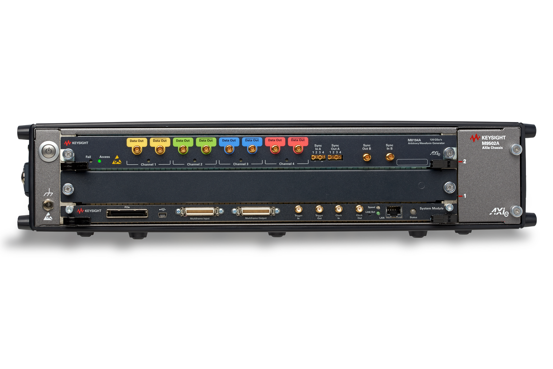
M8190A 任意波形发生器 详细指标
Modular AXI Waveform and Function Generators
An AWG is the most versatile signal scenario generator possible.
Capabilities such as easy switching between
14-bit output at
8 GSa/s and 12-bit output at 12 GSa/s help you handle multiple
条件:signals. You can switch between them as needed through software commands. Some applications call for Multi-channel support. The M8192 AXIe module can be plugged into the chassis ensuring alignment up to 12-channels.
Because every application calls for different signal character -
istics, the Keysight M8190A also contains three amplifiers that
are optimized for I/Q signals, IF/RF output, or clean time-domain
– Single-ended or differential output
700 mVpp, single-ended
– Offset –20 mV ...
+20 mV
– Adjustable differential offset
– Up to 5 GHz
2.0 Vpp, single-ended
– Amplitude 500 mVpp …
1.0 Vpp
–1.0 V to +3.3 V
– Transition times (20/80)
< 60 ps
Best SFDR and HD High bandwidth high voltage Time domain measurements
Highly realistic testing often requires long play times and long signal scenarios
For example
2 GSa of memory combined with advanced
sequencing capabilities allow you to use the memory efficiently
条件:WLAN; SystemVue, MATLAB, LabView or your own routines written in C++, C# or Visual Basic.
Direct access to individual memory segments is possible in real
time through the dynamic sequence control input. You can create
waveforms and download them into the M8190A using software
applications such as Signal Studio Pulse Builder, Multi-tone and
For sensitive applications, memory storage is not persistent:
Memory contents are volatile and are erased when power is turned off.
N7617B Signal Studio
N7621B Signal Studio
N5990A Test automation
N5990A Test automation
software for HDMI
81199A Wideband
N7620B Pulse Builder
33503A BenchLink
Assemble the best configuration for your application
The typical test setup shown to the right covers high RF applications up to 40 or 60 GHz. In this case the M8190A generates differential
I/Q signals that are sent to an upconverter such as the Keysight PSG signal generator. The M8190A is packaged in the AXIe form factor,
which reduces 系统尺寸, 重量和 footprint
The block diagrams shown to the right illustrate configurations for I/Q modulation and direct IF/RF output. The M8190A supports direct
generation of IF signals: Because this is done digitally, signal quality is outstanding. The instrument provides an analog bandwidth of
5 GHz; if higher output frequency is needed a mixer must be added to the configuration.
IF/RF up to 5 GHz
modulation BW (8 GHz
with doublet mode) data up to 6 Gb/s
条件:Generate multi-level signals with programmable ISI and jitter up to 6 Gb/s.
Modulation BW up to 2 GHz RF up to 44 GHz
The M8190A is equipped to ensure flexible modifications to fit
new distortion requirements by simply adapting the waveform itself. You can easily mimic analog imperfections that occur in real-world environments by using mathematical description in tools such as MATLAB. This minimizes the need for additional
hardware while preserving the ability to create realistic signal
条件:Jitter and noise cause misalignment of edges and levels, resulting in data errors.
Push radar and electronic warfare designs farther with highly realistic signal scenarios
条件:In aerospace and defense, technology is evolving to wider bandwidths without compromising on resolution.
The foundation is digital technology, which is becoming more prevalent because it provides advantages such as reduced size, lower power requirements, better calibration and faster volume scans.
When developing radar systems, real-life testing is very expen -
sive. Simulations with highly realistic signals help reduce the cost
of system testing. The Keysight M8190A addresses these needs
with three key capabilities: wide bandwidth, high resolution and
条件:under sequencer control. Even complex operations such as frequency sweep are possible. Streaming functionality is available for infinite playtime. Endless scenarios can be played.
ory. An example might be NPR measurement where thousands of waveform combinations are required to cover all test cases and the signal must not be interrupted.
Real-time digital signal processing with Keysight proprietary ASIC
Digital up-conversion takes testing one step further. The wide
bandwidth allows generating the IF signal directly. The IQ data
will be upconverted digitally in hardware which gives you best
signal quality in the desired frequency range. The frequency resolution is very precise with sample clock down to the picosec - ond range. In addition efficient memory usage allows to extend the playtime by up to 1 million times. For example for a radar
signal the waveform needs to be stored only once and amplitude,
frequency and phase are stored independently. Precise carrier
frequency, phase and amplitude settings is possible in real-time
While up to 2G Samples of waveform memory and a powerful
sequencing engine provide sufficient playtime for most cases,
there are some applications, such as radar scenario simulations,
where playtimes in the order of several minutes are required.
In another class of applications, the number of possible waveform
segments is too large to be pre-loaded into the waveform mem -
To address these applications, the M8190A offers the unique
capability to download waveforms into portions of the waveform
memory while the generator is running. In its simplest form, two waveform segments (A and B) are defined and while the generator outputs segment A repetitively, software can update segment B. Using a software command, the generator switches
over to output segment B and while B is output, segment A can
be overwritten and so on. This functionality is often referred to as
Taking this a step further, the waveform memory can be split up
into a certain number (>=
5) of waveform segments which are
linked together as a ring buffer (i.e. A � B � C � D � E � A
条件:� B, etc.). The generator sequentially outputs each waveform segment and as soon as it proceeds to the next one, the software loads a new waveform into this segment. This mode of operation is referred to as streaming.
In continuous streaming mode, the generator proceeds from one segment to the next without any pauses. Obviously, this mode requires the software and controlling PC to deliver new waveform segments fast enough to keep up with the rate that the
条件:for waveform download can be dramatically reduced (resp. the output bandwidth during pulse on-time increased).
Mode, because the baseband information can be provided at a much lower sample rate – independent of the carrier frequency.
In triggered streaming mode, the generator proceeds to the next segment upon an internal or external trigger event. This mode is particularly useful for pulsed radar simulations, where short pulses are interleaved with long pauses with a certain on/
off ratio. Depending on the on/off ratio, the required throughput
Streaming works best in conjunction with Digital Up-conversion
Waveform data for streaming can be retrieved from a number of
– Harddisk – typically a fast RAID drive or Solid State Drive
(SSD), which offers sufficient data throughput for continuous
条件:waveforms that are available in PC memory. User software can select which waveform is used at which point in time.
– Algorithmically generated – typically a pre-calculated set of
Thoughput and achievable bandwidth
条件:This is the maximum that can be achieved in DUC mode – depending on the on/off ratio of the signal (please refer to publication no. 5991-3937EN).
For continuous streaming, the hardware and software on the controlling PC must be able to deliver data fast enough to keep up with waveform generation. On a high-end PC, a thoughput of 500 – 600 MByte/s are achievable. In Digital Up-conversion
mode, this corresponds to a modulation bandwidth of 125 to
150 MHz (4 bytes per I/Q sample pair). In triggered streaming
mode, approx.
2 GHz modulation bandwidth can be achieved.
The memory ping-pong and streaming functionality is available
starting with M8190A firmware Rev.
3.0. An example program in
C++ (both source and executable) is provided with the firmware
PC (external or embedded controller)
PCIe x4 Gen2
条件:High numbered digital modulations transport more data in the same bandwidth, but tend to produce inaccurate levels and phase angles. Detailed testing becomes very important.
As a result, it is necessary to create high-quality signals with
14-bit resolution SFDR less than
–90 dBc. This excellent SFDR
ensures that tones stand out from distortion, even with hundreds
of tones. The
2 GSa memory ensures that you can store more
than one signal scenario and simply switch between segments via
direct memory access and the dynamic sequence control input
条件:bandwidth gives you enough headroom to test and address next-generation modulation schemes.
The M8190A gives you the versatility to define new signals—pro -
prietary, next-generation and beyond. The
5 GHz modulation
Build a strong foundation for highly reliable satellite communications
Accurate emulation of transmissions—from ground station to airborne transceiver to distant ground
Bundles including AXIe chassis are available under
– M8190A -BU1 5 slot chassis, with embedded PC 16 GB RAM and Windows Embedded Standard 7 operating system
64 bit
– M8190A -BU2 2 slot chassis (connectivity accessories will be added automatically - choice between desktop and laptop cabling)
– M8190S Multichannel Arbitrary Waveform Generator System (4- &
8 channels are selectable)
M8190A Option Software upgradeable Comment
1 channel 001 MUST order either
001 or 002 or LPN (requires
customer-provided external clock source)2 channel
002
2 channels with low phase noise LPN
14 bit/8 GSa/s 1 14B X MUST order either
14B or 12G or both options
Additional DC and AC amplifier
1 AMP X
Digital up-conversion to carrier frequency
1 DUC X
Upgrade from 128 MSa to 2 GSa memory per
channel 02G X 2 channel version requires Option 02G (quantity
2)
Fast switching
1 FSW X Fast switching for 12 GSa/s
ISO 17025
1A7 Calibration options
M8190A-801 Microwave phase matched balun
6.5 GHz, max SMA jack
M8190A-805 Low pass filter, 2800 MHz, max SMA, VLF
2850+
M8190A-806 Low pass filter, 3900 MHZ max SMA, VLF
3800+
M8190A-810 Cable assembly coaxial–50 Ω, SMA to SMA
457 mm length
M8190A-811 Cable assembly coaxial–50 Ω, SMA to SMA
1220 mm length
M8190A-815 Dynamic control input cable
M8190A-820 Connector-RF, SMA termination, plug straight, 50 Ω, 12.4 GHz
0.5 W
Challenge the Boundaries of Test Keysight Modular Products
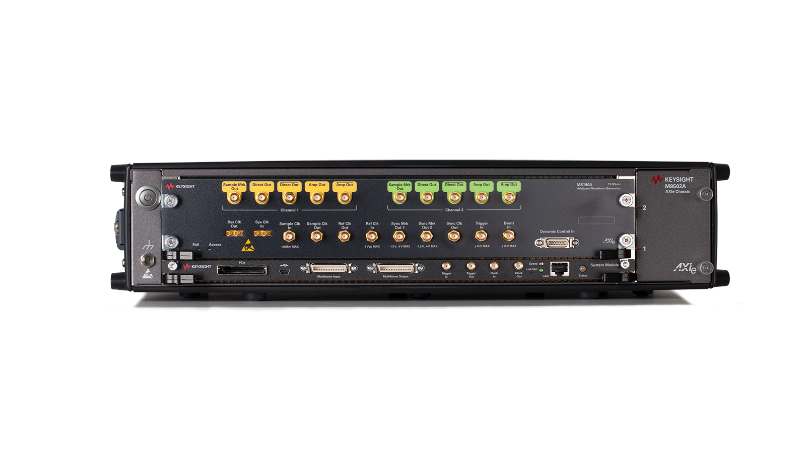
条件:Five slot AXle chassis with two M8190A AWG; can contain an embedded controller.
Two slot AXIe chassis with M8190A AWG.
The chassis can be used on the bench or in a rack, occupying only
4U of rack space. Keysight computer I/O cards are also available
– M9502A-U20
2-slot AXIe chassis with USB option
– M9505A-U20
5-slot AXIe chassis with USB option
– M9048A: PCIe desktop card adapter Gen
2 x8
– Y1200B: x4 – x8 PCIe cable
– Y1202A: x8 – x8 PCIe cable
– M9537A: Embedded AXIe controller
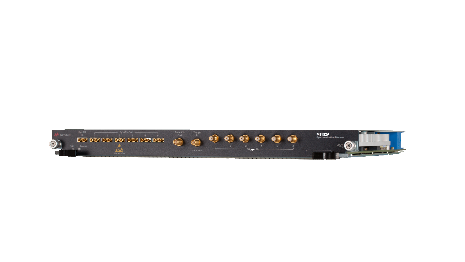
– M8192A Multi-Channel Synchronization Module for M8190A
The M8190A is a modular instrument packaged in the AXIe
form factor. AXIe is a new open standard for high-performance,
modular instrumentation, and incorporates the best features of
other modular formats including VXIbus, LXI and PXI. Keysight
offers a line of scalable chassis in this powerful format. Along
with controller options, these AXIe chassis can form the basis of
高-性能, AXIe-based 测试 systems
条件:These include an embedded AXIe system module that does not occupy a module slot. In addition, an AXIe controller is an entire system that can control the AWG. This controller consumes one module slot in the chassis.
Two form factors are available: two-slot and five-slot chassis.
Digital to analog converter
– Option: –14B Resolution
14 bit
Sample rate
125 MSa/s to 8 GSa/s
– Option: –12G Resolution
12 bit
Sample rate
125 MSa/s to 12 GSa/s
Sin (x)/x roll-off (mathematically calculated)
– Option: –14B Sin (x)/x (–1 dB)
2.1 GHz at 8 GSa/s
Sin (x)/x (–3 dB)
3.5 GHz at 8 GSa/s
– Option: –12G Sin (x)/x (–1 dB)
3.1 GHz at 12 GSa/s
Sin (x)/x (–3 dB)
5.3 GHz at 12 GSa/s
条件:Connector type SMA 1. Determines the minimum time needed to switch between selected segments in sequence mode. 2. Unused output must be terminated with 50 Ω to GND. 3. Doublet mode does not allow DC signal generation.
Effective output frequency (f max is determined as f Sa,max /2.5)
– Option: –14B fmax =
3.2 GHz
– Option: –12G fmax =
4.8 GHz
Effective frequency switching time
1
– Option: –14B with or without FSW 313 ps (=
1/ fmax )
– Option: –12G without FSW
105 µs to 210 µs
– Option: –12G with FSW 208 ps (=
1/fmax )
Direct out1/direct out2
Type of output Single-ended
2 or differential, DC-coupled
Skew between normal and complement outputs
0 ps (nom)
Skew accuracy between normal and complement outputs
± 5 ps (typ)
Amplitude control Specified into
50 Ω
– Range, single-ended (DNRZ/NRZ mode)
350 mVp-p to 700 mVp-p
– DC accuracy, offset = 0 V (DNRZ/NRZ mode) 3 ± (1.5% +
15 mV) (spec)
Offset –20 mV to + 20 mV, single-ended into
50 Ω
Offset resolution
60 µV (nom)
DC offset accuracy
± 10 mV (spec)
Common mode offset and differential offset is seperately adjustable
条件:SFDR in 14 bit mode 2, 4 (excluding harmonic distortion) In band performance:
Bandwidth (3 dB)
3.0 GHz (typ)
Bandwidth (5 dB)
5.0 GHz (typ)
Harmonic distortion 7.2 GSa/s 2, 4 –72 dBc (typ, fout =
100 MHz)
–68 dBc (typ), f out = 10 MHz ...
200 MHz, measured DC to 3 GHz
–60 dBc (typ) , f out = 200 MHz ...
3000 MHz, measured DC to 3 GHz
Harmonic distortion 12 GSa/s 3, 4 –54 dBc (typ) f out =
100 MHz
–50 dBc (typ) f out = 10 MHz ...
5000 MHz, measured DC to 5 GHz
–90 dBc (typ), fout =
100 MHz, measured DC to 2 GHz
–80 dBc (typ), fout =
10 MHz…500 MHz, measured DC to 500 MHz
–76 dBc (typ), fout =
500 MHz…1 GHz, measured DC to 1 GHz
–68 dBc (typ), fout =
1 GHz…2 GHz, measured DC to 2 GHz
–62 dBc (typ), fout =
2 GHz…3 GHz, measured DC to 3 GHz
条件:SFDR in 12 bit mode 3, 4 (excluding harmonic distortion) In band performance:
–80 dBc (typ), fout =
10 MHz…500 MHz, measured DC to 1.5 GHz
–73 dBc (typ), fout =
500 MHz…1 GHz, measured DC to 3 GHz
–68 dBc (typ), fout =
1 GHz…2 GHz, measured DC to 3 GHz
–62 dBc (typ), fout =
2 GHz…3 GHz, measured DC to 3 GHz
–90 dBc (typ), fout =
100 MHz, measured DC to 2 GHz
–80 dBc (typ), fout =
10 MHz…500 MHz, measured DC to 500 MHz
–78 dBc (typ), fout =
500 MHz…1 GHz, measured DC to 1 GHz
–73 dBc (typ), fout =
1 GHz…2 GHz, measured DC to 2 GHz
–68 dBc (typ), fout =
2 GHz…3 GHz, measured DC to 3 GHz
–60 dBc (typ), fout =
3 GHz…5 GHz, measured DC to 5 GHz
条件:1. tr bandwidth: BW = 0.25/t r.
2. SCLK = 7.2 GSa/s, amplitude = 700 mV p-p, double NRZ mode, excluding f Sa – 2 * fout, fSa – 3 * fout .
3. SCLK = 12 GSa/s, amplitude = 700 mVp-p, double NRZ mode, excluding f Sa – 2 * fout, fSa – 3* f out .
4. Measured with a balun such as the HL9402 from Hyperlabs plus 10 dB attenuator.
–80 dBc (typ), fout =
10 MHz…500 MHz, measured DC to 1.5 GHz
–73 dBc (typ), fout =
500 MHz…1 GHz, measured DC to 3 GHz
–68 dBc (typ), fout =
1 GHz…2 GHz, measured DC to 5 GHz
–64 dBc (typ), fout =
2 GHz…3 GHz, measured DC to 5 GHz
–60 dBc (typ), fout =
3 GHz…5 GHz, measured DC to 5 GHz
Two-tone IMD 2 TTIMD = –73 dBc (typ), f out1 = 499.5 MHz, f out2 =
500.5 MHz
Bandwidth See frequency plot (measured)
8 GHz/12 GHz, single ended
Harmonics 14 bit doublet mode 1 8 GSa/s fout = 5400 MHz ... 6500 MHz measured
5.4 GHz to 6.5 GHz, no harmonics in this range
Harmonics 12 bit doublet mode 2 12 GSa/s fout = 8100 MHz ... 9900 MHz, measured
8.1 GHz to 9.9 GHz, no harmonics in this range
SFDR in 14 bit doublet mode
8 GSa/s
–48 dBc (typ) f out = 5400 MHz ... 6500 MHz, measured
5.4 GHz to 6.5 GHz, Single ended
SFDR in 12 bit doublet mode
12 GSa/s
条件:1. SCLK = 8 GSa/s, amplitude = 700 mV p-p, double NRZ mode, excluding f Sa – 2 * fout, fSa – 3 * fout .
2. SCLK = 12 GSa/s, amplitude = 700 mV p-p .
–44 dBc (typ) f out = 8100 MHz ... 9900 MHz, measured
8.1 GHz to 9.9 GHz, Single ended
0 500 1000 1500 2000 2500 3000
3500
14 Bit / 7.2GSa/s
ENOB 14 bit ; 7.2 GSa/s 0 1000 2000 3000 4000 5000 6000
12 Bit / 12GSa/s
fOut [MHz] 12 bit
12 GSa/s
0 200 400 600 800 1000
1200
fOut [MHz] 14 bit
2.5 GSa/s
条件:Two selectable output paths per channel are available when Option AMP is installed: 1) DC output path 2) AC output path.
Eye pattern with amplitude
1000 mV with 0 V offset.
Amp out1/amp out2
条件:Connector type SMA 1. Unused output must be terminated with 50 Ω to the termination voltage. 2. Termination voltage = 0 V; adjusted at 23 °C ambient temperature, amplitude reduces by 2 mV/°C (typ) for ambient temperature above 23 °C, amplitude increases by 5 mV/°C (typ) for ambient temperature below 23 °C 3.
3. Termination voltage window: offset ± 1 V.
4. Termination voltage = 0 V.
5. PRBS 211 – 1, fSa = 12 GSa/s, data rate = 3 Gb/s, triggered on sample clock out, NRZ mode.
Output type Single-ended
1 or differential, DC-coupled
Amplitude 500 mVpp to 1.0 Vpp, single-ended into
50 Ω
Amplitude resolution
300 µV (nom)
DC amplitude accuracy ± (2.5% + 10 mV) (nom)
2
Voltage window –1.0 V to + 3.3 V 3, single-ended into
50 Ω
Offset resolution
600 µV (nom)
DC offset accuracy ± 2.5% ± 10 mV (typ) ± 4% of amplitude (typ)
4
Termination voltage window –1.5 V to + 3.5 V
3
Termination voltage resolution
300 µV (nom)
Skew between normal and complement outputs
0 ps (nom)
Skew accuracy between normal and complement outputs
± 5 ps (typ)
Rise/fall time (20 to 80%) < 60 ps (typ)
5
Jitter (peak-peak) 15 ps (typ)
5
Front-panel marking: amp out1 for channel 1; amp out2 for channel
2
Amplitude
200 mVpp to 2.0 Vpp
Amplitude resolution
0.25 dB (nom)
Amplitude accuracy ± 0.5 dB
1 (typ)
Bandwidth (3 dB)
50 MHz to 5 GHz (typ)
Harmonic distortion 2 < –39 dBc (typ), f out =
375 MHz, measured DC to 3 GHz
< –37 dBc (typ), fout = 100 MHz … 3000 MHz, measured
100 MHz to 3 GHz
Harmonic distortion 3 < –39 dBc (typ) f out =
375 MHz, measured DC to 5 GHz
< –37 dBc (typ) fout = 100 MHz ...
5000 MHz, measured DC to 5 GHz
SFDR in 14 bit mode
2 (excluding harmonic
< –60 dBc (typ), f out = 100 MHz … 2000 MHz, measured
100 MHz to 3000 MHz
< –56 dBc (typ), f out = 2000 MHz … 3000 MHz, measured
100 MHz to 3000 MHz
SFDR in 12 bit mode
3 (excluding harmonic
条件:Connector type SMA 1. 500 MHz sine wave. 2. SCLK = 7.2 GSa/s, amplitude = 1 V p-p, 14 bit mode, double NRZ mode, excluding f Sa - 2*f out, fSa - 3*fout . 3. SCLK = 12 GSa/s, amplitude = 1 V p-p, 12 bit mode, double NRZ mode, excluding f Sa - 2*f out, fSa - 3*fout .
4. SCLK = 12 GSa/s, amplitude = 1 V p-p; normalized to 100 MHz; 12 bit mode, includes sin (x)/x compensation.
5. SFDR numbers for interpolation mode are the same as the SFDR numbers for 14 bit mode. For further specification please see the digital up-conversion
< –60 dBc (typ), f out = 100 MHz … 2000 MHz, measured
100 MHz to 5000 MHz
< –56 dBc (typ), f out = 2000 MHz … 3000 MHz, measured
100 MHz to 5000 MHz
< –50 dBc (typ), f out = 3000 MHz … 5000 MHz, measured
100 MHz to 5000 MHz
Amplitude flatness 4 100 MHz to 1 GHz (typ), +
1.5 dB to –0.5 dB
100 MHz to 4 GHz (typ)
± 0.1 dB with calibration / pre-distortion
1 GHz to 4 GHz (typ), –2 dB to +
3 dB
Two-tone IMD 2 TTIMD = –46 dBc (typ), f out1 = 999.5 MHz, f out2 =
1000.5 MHz
Sync marker: Single ended
Sync marker out1/sync marker out
2
Output impedance
50 Ω (nom)
Timing resolution 1 N sample clock cycles (N = 64 in 12 bit mode; N =
48 in 14 bit mode)
– Voltage window
–0.5 V to 2.0 V
– Amplitude
200 mVpp to 2.0 Vpp
– Accuracy ± (10% +
25 mV) (typ)
Rise/fall time (20 to 80%)
150 ps (nom)
Width 1 User-defined in multiples of N sample clock cycles (N = 64 in 12 bit mode; N =
48 in 14
Sample marker out1/sample marker out
2
Timing resolution
1 sample clock cycle
条件:Connector type SMA 1. See characteristics digital up-conversion if interpolation is enabled.
– Voltage window
–0.5 V to 2.0 V
– Amplitude
200 mVpp to 2.0 Vpp
– Accuracy ± (10% +
25 mV) (typ)
Rise/fall time (20 to 80%)
150 ps (nom)
Width
49 sample clocks in 12 bit mode
40 sample clocks in 14 bit mode
Random jitter
5 ps RMS (typ)
Polarity Selectable positive or negative
Drive Selectable channel 1, channel
2 or both
Input Impedance
1 kΩ or 50 Ω (nom), DC coupled
– 12 bit mode Sample clock output frequency divided by
320
– 14 bit mode Sample clock output frequency divided by
240
Asynchronous timing between trigger/gate and sync clock output
1.1 * sync clock period
Synchronous timing between trigger/gate input and sync clock output
五、See set-up and hold timing under timing Specifications
A common dynamic control input for both channels is provided on the front panel. The user can select, if the dynamic control input
affects none, only channel 1/channel
2 only, or both channels. A detailed description of the dynamic control input including timing
diagram and pin assignment is shown in the M8190A User’s Guide.
Input signals Data[0..12]_In + Data_Select + Load
1
Internal data width
19 bit, multiplexed using Data_Select
Data_Select Data_Select = Low: Data[0..12] = Data[0..12]_In
Data_Select = High: Data[13..18] = Data[0..5]_In
Number of addressable segments or sequences 219 = 524
288
Data rate DC to 1 MHz
Set-up time
3.0 ns (`Data[0..12]_In, `Data_Select’ to rising edge of `Load’)
Hold time
0.0 ns (rising edge of `Load’ to `Data[0..12]_In, `Data_Select’)
Minimum 3 latency
4 Dynamic control input to direct out
– 12 bit mode
27520 sample clock cycles (meas)
– 14 bit mode
20640 sample clock cycles (meas)
条件:1. Data[0…12]’_In and `Data_Select’ will be stored on rising edge of `Load signal.’
2. Manufacturer Part Number: N10220-52B2PC. Manufacturer: 3M.
3. As the current segment (or sequence or scenario) is always completed, the total latency is determined by the duration of the segment (or sequence or
scenario). See characteristics of digital up-conversion if interpolation is enabled.
4. See characteristics digital up-conversion if interpolation is enabled.
– High level
+1.6 V to +3.6 V
Impedance Internal
1 kΩ pull-down resistor to GND
Connector 20 pin mini D ribbon (MDR) connector 2, cable Option
815
条件:Trigger/Gate Input, Event, Input or Dynamic Control must be synchronous to the Sync Clock Output.
The M8190A can operate synchronously or asynchronously. Synchronous operation must be selected to achieve minimum delay
uncertainty between Trigger Input, Event, Input or Dynamic Control Input and Direct Out or Marker Out. For synchronous operation
– Trigger/gate in to rising edge of sync clock out
10.5 ns (typ)
– Event in to rising edge of sync clock out
10.5 ns (typ)
– Rising edge of sync clock out to trigger/gate in –7.5 ns (typ)
– Rising edge of sync clock out to event in –7.5 ns (typ)
Delay in 12 bit mode
– Trigger/event in to direct/DC/AC out 10240 external sample clock cycles + 0.5 internal
1 sample clock cycles (nom)
– Sync marker to direct/DC/AC out 0.5 internal 1 sample clock cycles - 4.9 ns (nom) (fSa >=
6.4 GSa/s)
0.5 internal 1 sample clock cycles - 8.0 ns (nom) (fSa <
6.4 GSa/s)
Delay in 14 bit mode
– Trigger/event in to direct/DC/AC out 7680 external sample clock cycles + 0.5 internal
1 sample clock cycles (nom)
– Sync marker to direct/DC/AC out 0.5 internal 1 sample clock cycles - 4.9 ns (nom) (fSa >=
4.8 GSa/s)
0.5 internal 1 sample clock cycles - 8.0 ns (nom) (fSa <
4.8 GSa/s)
Sample marker to direct/DC/AC out 0.5 internal
1 sample clock cycles - 1.3 ns (nom)
条件:1. Internal sample clock cycles. For definition of ‘Internal sample clock cycles’ refer to sample clock outputs specification.
2. The delay accuracy in synchronous mode is equal to the peak-peak jitter between sync clock output and direct out.
Note: Timing characteristics of DUC, see digital up-conversion (DuC) chapter.
Asynchronous mode
64 external sample clocks in 12 bit mode
48 external sample clocks in 14 bit mode
Synchronous mode 10 ps (typ)
2
In order to compensate for e.g. external cable length differences as well as the initial skew, channel 1 and channel
2 can be inde -
pendently delayed with a very high timing resolution
Setting the variable delay of channel
1 to 10 ps has following effect:
– Direct out1 (or amp out1, if selected) and sample marker out1 are delayed by
10 ps with respect to following signals: sample
clock out, sync marker out1, sync marker out2, direct out2 (or amp out2, if selected), trigger/gate input, event input
Note: Modifying the variable delay of one channel always affects the delay of the analog output AND the sample marker of that
条件:first step the coarse delay to the optimum position. In the second step, use the fine delay to perfectly align both channels.
The variable delay is split into two delay elements: 1. Fine delay
2. Coarse delay
The variable delay is the sum of fine delay and coarse delay. If a de-skew between channel 1 and channel
2 is needed, adjust in the
– fSa ≥ 6.25 GSa/s
0 ps to 10.030 ns
– 2.5 GSa/s ≤ f Sa < 6.25 GSa/s
0 ps to 10.060 ns
– fSa < 2.5 GSa/s
0 ps to 10.150 ns
The fine delay is independently adjustable for channel 1 and channel
2
– fSa ≥
6.25 GSa/s – 0 ps to 30 ps
– 2.5 GSa/s ≤ f Sa <
6.25 GSa/s – 0 ps to 60 ps
– fSa <
2.5 GSa/s – 0 ps to 150 ps
条件:1. For definition of “internal sample clock cycles”, refer to sample clock output specification.
Note for delay in interpolation mode: Please see digital up-conversion specification.
– fSa ≥ 6.25 GSa/s
± 10 ps (typ)
– 2.5 GSa/s ≤ f Sa < 6.25 GSa/s
± 20 ps (typ)
– fSa < 2.5 GSa/s
± 20 ps (typ)
The coarse delay is independently adjustable for channel 1 and channel
2
Delay range
0 ps to 10 ns, variable
– 2.5 GSa/s ≤ f Sa < 6.25 GSa/s
20 ps
– fSa < 2.5 GSa/s
50 ps
条件:1. Coupling on, same amplifier path is selected for channel 1 and channel 2.
– fSa ≥ 6.25 GSa/s
± 20 ps (typ)
– 2.5 GSa/s ≤ f Sa < 6.25 GSa/s
± 20 ps (typ)
– fSa < 2.5 GSa/s
± 50 ps (typ)
When the variable delay is set to 0 ps, the channels operate in coupled mode and the same amplifier path for both channels is select -
ed, the initial skew between channel 1 and channel 2 is
0 ps.
Initial skew between channel 1 and channel
2
Source Internal backplane
100 MHz
– Stability
± 20 ppm (typ.) (see M9502A/M9595A Data Sheet)
Source Internal Oven-Controlled Reference Oscillator
– Accuracy
± 0.2 ppm (typ.)
– Stability
± 0.6 ppm (typ.)
– Aging
± 0.3 ppm per year (typ.)
– Phase noise –95 dBc/Hz at 10 Hz
–125 dBc/Hz at 100 Hz offset (typ.)
Phase noise at offsets > 100 Hz (refer to phase noise plots on page
30)
– Amplitude 1 Vpp into
50 Ω (nom)
– Source impedance
50 Ω, AC coupled (nom)
Input frequencies Selectable
1 MHz to 200 MHz, in steps of 1 MHz
Frequency resolution
1 MHz
Input level
100 mVpp to 2 Vpp
Impedance
50 Ω, AC coupled (nom)
条件:Impedance 50 Ω nominal, AC coupled
– 14 bit mode Sample clock divided by 48 (sample clock source is always channel
1)
– 12 bit mode Sample clock divided by 64 (sample clock source is always channel
1)
– Interpolation mode Sample clock divided by (24 x interpolation factor)
Output amplitude 1.0 Vpp (nom) into
50 Ω
条件:different clock sources are selected for the channels, both channels operate entirely independently with respect to sample rate and sequencing.
The two channel instrument (Option 002) offers the flexibility to independently select the sample clock sources for channel one and channel two. If
Frequency
125 MHz to 12 GHz
Frequency resolution 15 digits, e.g.
10 µHz at 1 GHz
Phase noise 1 fSa = 1 GHz < –110 dBc/Hz (typ) at 10 kHz offset, fout = 125 MHz
2
fSa = 8 GHz < –105 dBc/Hz (typ) at 10 kHz offset, fout = 1.0 GHz
2
fSa = 12 GHz < –105 dBc/Hz (typ) at 10 kHz offset, fout =
1.5 GHz
条件:Connector type SMA 1. The sample clock output is derived from the internal sample clock f Sa, i. For fSa, i = 500 MSa/s…1 GSa/s the sample clock output is twice of f Sa, i. For fSa, I = 250 MSa/s … 500 MSa/s the sample clock output is four times f Sa, i. For fSa, i = 125 MSa/s … 250 MSa/s the sample clock output is eight times f Sa, i. 2. Measured at “data out”.
Low Phase Noise clock input (only with option LPN)
Frequency range
1 GHz to 12 GHz
Input power range
+0 dBm to +7 dBm
Input impedance
50 Ω nom, AC coupled
Frequency range
1 GHz to 12 GHz
Input power range +0 dBm to +
7 dBm
Input impedance
50 Ω nom, AC coupled
– Configuring the instrument for low phase noise mode forces the channels to operate in coupled and reduced noise floor mode. In
Phase noise plot with internal sample clock
7.2 GSa/s, direct
output measured with balun
Phase noise plot with external sample clock
7.2 GSa/s, direct
output measured with balun
Phase noise plot with internal sample clock
12 GSa/s, direct
output measured with balun
Phase noise plot with external sample clock
12 GSa/s, direct
These plots show the typical phase noise using the delay adjustment
条件:measured with balun and reduced noise floor.
measured with balun and reduced noise floor.
measured with balun and reduced noise floor.
measured with balun and reduced noise floor.
Phase noise with internal sample clock
7.2 GSa/s, direct out
Phase noise with external sample clock
7.2 GSa/s, direct out
Phase noise with internal sample clock
12 GSa/s, direct out
Phase noise with external sample clock
12 GSa/s, direct out
These plots show the typical phase noise without using the delay adjustment
条件:tor phase noise performance. With option LPN a customer-sup -
Option LPN significantly improves the arbitrary waveform genera -
plied external synthesizer (1-12 GHz range) must be connected.
The measurements in the following graph were performed using a Keysight proprietary external oscillator and measured using a
Keysight E5052B signal source analyzer.
-170
-160
-150
-140
-130
-120
-110
-100
-90
100 1000 10000 100000 1000000 10000000
100000000
Offset frequency (Hz) 187,5 MHz Sine wave - Sample clock 7,2GHz 375 MHz Sine wave - Sample clock 7,2GHz 750 MHz Sine wave - Sample clock
7,2GHz
1500 MHz Sine wave - Sample clock
7,2GHz
3000 MHz Sine wave - Sample clock 7,2GHz3000 MHz Sine wave - Sample clock
7,2GHz
This plot show the typical phase noise with the low phase noise option (opt. LPN)
External sample clock source M8190A (LPN Opt.)
条件:to the sample clock input as to be used as the sample clock of the M8190A.
The following table shows which sample clock out routings are possible if coupling is on.
The following table shows which sample clock out routings are possible if coupling is off.
The source for the sample clock output can be either the internal synthesizer or the sample clock input. The source for the sample
clock output can be independently selected from the sample clock. For example, it is possible to operate the sample clock output from
the internal synthesizer at f 1 to clock the DUT; as an example, f1 may be divided by two by the DUT. In this case, f
1/2 can be connected
External clock Internal clock 12 bit 14 bit 12 bit
14 bit
Channel 2 External clock
12 bit External clock — — —
14 bit — External clock — —
Internal clock
12 bit — — Internal clock —
14 bit — — — Internal clock
External clock Internal clock 12 bit 14 bit 12 bit
14 bit
Channel 2 Channel
2 operate
with external clock
12 bit External or internal clock
External or internal clock
14 bit External or internal clock
with internal clock
12 bit External or internal clock
— 14 bit External or internal
条件:Connector SMA 1. The sample clock output is derived from the internal sample clock f Sa, i. For fSa, i = 500 MSa/s…1 GSa/s the sample clock output is twice of f Sa, i. For fSa, I = 250 MSa/s … 500 MSa/s the sample clock output is four times f Sa, i. For fSa, i = 125 MSa/s … 250 MSa/s the sample clock output is eight times f Sa, i.
Source Selectable, internal synthesizer or sample clock input
Frequency range
1 to 12 GHz
Output amplitude
400 mVpp (nom), fix
Input impedance
50 Ω (nom), AC coupled
Transition time (20 to 80%)
20 ps (typ)
条件:The two channel instrument (Option 002) has two distinct modes of operation: coupling = off and coupling = on.
Coupling between channel 1 and channel
2
– 通道 may run · 不同 sample 时钟速率
– The channels may run from the same clock source (internal or external)
– The channels may operate from different clock sources (internal or external)
– The channels are being started asynchronously
– Following parameters can be changed individually per channel:
– Start/stop (programming/programming complete)
– 12 bit or 14 bit mode (see limitations in table below)
– Dynamic sequencing on/off
– Following parameters can only be changed for both channels:
条件:The following table shows which mode combinations are available, if coupling is off.
External clock Internal clock 12 bit 14 bit 12 bit
14 bit
Channel 2 External clock
12 bit Available Available Available Available
14 bit Available A
以上指标摘自厂家官方数据手册,完整定义、测试条件与保证值口径以手册为准。完整指标、测试条件与定义口径请见产品页「软件和手册 | 白皮书」栏目中的官方数据手册。
是德科技 | KEYSIGHT · onetest 仪器资源库



 客服









 粤公网安备44030902003758