ONETEST 欢迎您
厂商登录 | 入驻
登录 | 注册 购物车 微信公众号


 客服


厂商登录


类似产品
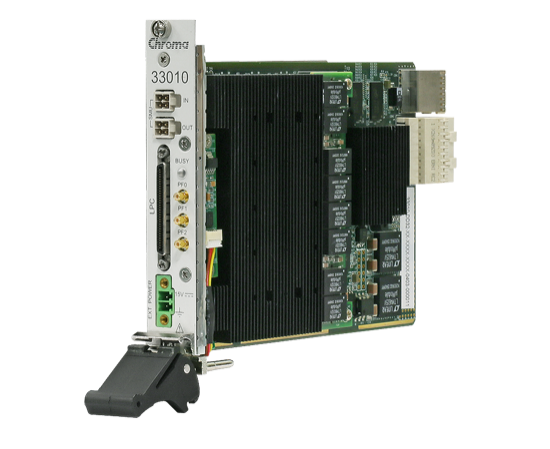
Chroma 33010 是一款高密度 100MHz PXIe 数字 IO 卡,用于各类数字与混合信号 IC 的特性分析、验证与测试。
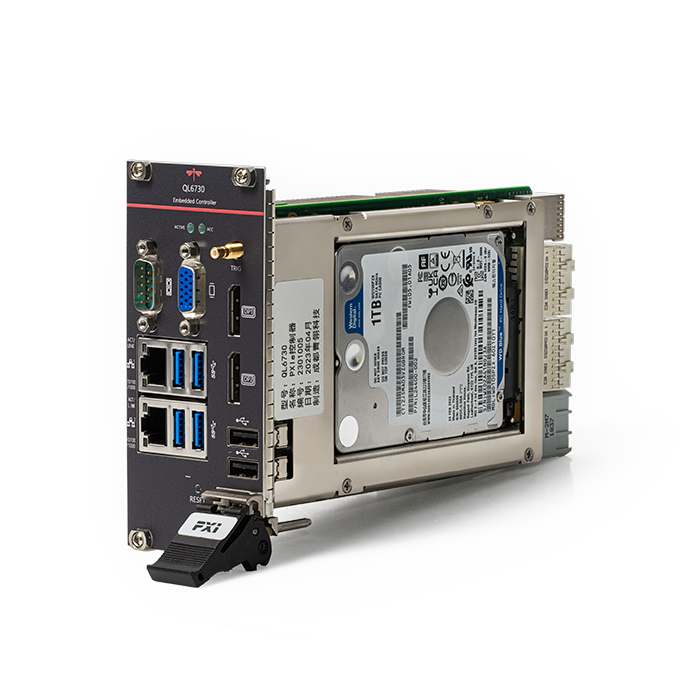
QL6730是一款基于PXIe架构的嵌入式控制器,内嵌Intel®高性能处理器,具有16GB/s的系统带宽、双千兆网口、4个USB3.0、2个USB2.0、2个DP、VGA和串行接口。
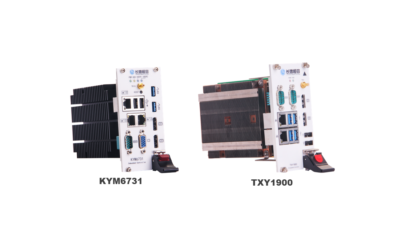
处理器:最高支持Intel® 第六代 Core™ i7处理器,4核8线程,最高可达2.8 GHz(8MB 2级缓存)操作系统:Windows 7, Windows 8, Windows 10, Linux控制中枢:采用Intel QM87 / Intel QM77平台控制中枢,支持丰富的IO接口集成显卡:针对工业级显示或工作站应用,以图形为中心的XTM从PCH获取显示端口用于支持显示;VGA 2048×1536像素 ,32-bit色彩@75Hz内存:DDR3- 1600MHz SDRAM标配4GB, 最高支持64GB存储:标配250G SATA SSD,可扩展; 支持2.5寸STSA硬盘、m.2固态硬盘、mSTSA硬盘
同厂商产品
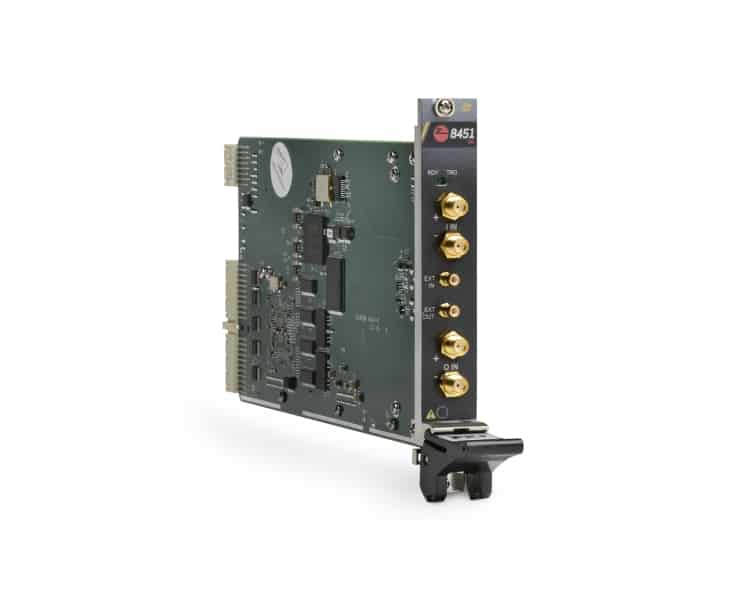
300MHz 差分 I/Q 数字化仪,双 ADC 400MS/s 同步采样、162.5MHz 无混叠带宽,内置实时 DDC 与 512MiB 存储。
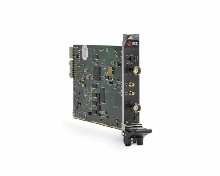
双通道 PXIe 任意波形发生器,200MS/s 14bit、14Vpp 入 50Ω,四档贝塞尔滤波,DDS 时钟 200S/s 至 200MS/s。

10MHz 至 6GHz 的 PXIe 射频开关与多路复用模块系列,隔离度 >85dB、插入损耗
- «
- 1
- »
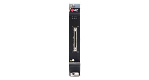
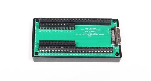
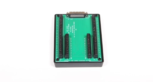

z482 12通道 200Mbps PXIe数字IO模块|LitePoint (停产)
参考价格 :
产品描述
详细指标
软件和手册|白皮书
购买渠道
选件
问大家
视频
测评
口碑
系统与解决方案
LitePoint
z482 12 通道数字 IO 模块
12 通道 · 每通道独立方向 · 每通道 PMU · 200Mbps · 通道间偏斜 ±500ps
产品简介
这块模块的定位不是「逻辑分析仪」,是**带测量能力的数字激励**。
给芯片的 SPI、I2C、MIPI 接口喂时序,同时用每通道的 PMU 验证引脚电平对不对、有没有对地短路、有没有悬空——12 个通道全部带 PMU 和远端感测,这一点是它跟普通数字 IO 卡的分界。
指标上:±500ps 的通道间偏斜,200Mbps 速率、100MHz 翻转率,32 组矢量集与 32 组时序集。
偏斜小意味着并行总线的建立/保持时间不会因为通道不同步而被吃掉——多线并行的接口测试,这一项决定测出来的是芯片问题还是板卡问题。
PMU 支持 DICV(驱流钳压)与 DVCI(驱压钳流)两种模式,覆盖电源引脚与信号引脚两类场景。
触发可接 PXI_TRIG[0:7]、PXI_STAR、PXIe_DSTAR 等总线,与同机箱射频模块同步。
12 引脚、每引脚带测量单元(PMU)的 PXIe 数字 IO 模块。
核心参数
• 通道数:12(全部带 PMU)
• 方向控制:每通道独立
• 远端感测:12 路,全 PMU 通道均支持
• 生成电压范围:-2V 至 6V
• 生成电压分辨率:100µV
• 输出电压摆幅:400mV 至 8V
• 精度:0.25% 读数 + 20mV
• 输出阻抗:50Ω 标称
• 最高数据率:200Mbps(每通道)
• 通道间偏斜:最大 ±500ps
• 矢量集 / 时序集:各 32 组
功能特性
• 12 通道全带 PMU:每个引脚既能驱动也能测电平与电流。
• 每通道独立方向:输入输出可混排,不用整组同步切换。
• ±500ps 通道偏斜:并行总线时序不被通道失配吃掉。
• 200Mbps 速率:满足高速接口的数字激励需求。
• DICV / DVCI 双模式:驱流钳压与驱压钳流,适配电源与信号引脚。
• 100µV 电平分辩:细粒度电平扫描,找输入阈值。
• 32 矢量集 / 32 时序集:多套测试图形切换,不用重载。
• PXIe 触发总线:与其他模块共用触发,激励与采集同步。
应用场景
• 芯片数字接口测试:SPI、I2C、MIPI 等接口的时序与电平验证。
• 引脚连通性检查:12 通道 PMU 逐脚测通断与短路。
• 上下电时序控制:多路使能信号的先后顺序编排。
• 射频模块控制:给 VSA/VSG 或开关模块发控制字。
• ATE 系统集成:作为数字侧激励与测量单元。
• 产线功能测试:接口功能与装配质量的快速判定。
• 研发协议调试:自定义图形激励,复现特定时序场景。
• 失效分析:引脚电平异常与悬空的定位。
资源下载
以上内容与指标均取自LitePoint(莱特波特)(LitePoint)官网该产品详情页与官方产品资料,未标注口径的为厂家公布值。
LitePoint · onetest 仪器资源库
LitePoint
z482 12 通道数字 IO 模块 详细指标
12 通道 · 每通道独立方向 · 每通道 PMU · 200Mbps · 通道间偏斜 ±500ps
详细指标
指标取自 LitePoint 官方技术规格书(PDF)。该型号官方已标注 Discontinued(停产),本站仍保留其页面与指标供存量系统参考。
引脚定义
• Number of data pins:12 pins of Pin Measurement unit (PMU) enabled
• Direction control of data pins:Per pin
• Number of remote sense pins:12 | All PMU-enabled pins have remote sense capability
• Generation Signal Type:Single-ended, ground reference
• Programmable generation voltage levels:Drive Voltage High Level (VIH) Drive Voltage High Level (VIL) Drive Termination Voltage (VT)
• Generation voltage range:-2 V to 6 V
• 精度:0.25% of value + 20 mV
• Generation voltage resolution:100 μV
• Generation voltage swing:400 mV to 8 V
• 输出阻抗:50 Ω | Nominal
• Maximum allowed DC drive per pin:± 50 mA | Nominal
• Data pin tristate control:Per pin, per cycle
• Pin power-on state:Drivers disabled, high impedance (tri-state)
• Output protection:The device can sustain a short to any voltage between -2 V and 6 V provided that you observe the maximum drive strength limitations
• Acquisition Signal Type:Single-ended, ground reference
• Programmable acquisition voltage levels:Compare High Level (VOH) Compare High Level (VOL) Voltage Termination (VT)
• Acquisition voltage threshold:-2 V to 7 V
• 精度(VOH, VOL):0.25% of value + 20 mV
• 精度(VT):0.25% of value + 20 mV
• Termination voltage resolution:600 μV
• Termination voltage range:0 V to 6.5 V
• Minimum detectable voltage swing:10 mV
• 输入阻抗:High Impedance or 50 Ω terminated into VT
• Input protection:The device can sustain a short to any voltage between -2 V and 6 V provided that you observe the maximum drive strength limitations
• Programmable levels:Current Source (IOH) Current Sink (IOL)
• Load:Range | Resolution
• Number of pins:6
• Programmable levels:Force voltage | HV = (VT + 1) x 2
• Force Voltage:Range | Accuracy
• Clamp Voltage Range High Side (VCH):-1.0 V to 6.0 V
• Clamp Voltage Range Low Side (VCL):-1.5 V to 5.0 V
• Termination Voltage (VT):-2.0 V to 6.0 V
• Programmable levels:Force voltage (FV) Force current (FI) Voltage clamp high (VCH) Voltage clamp low (VCL) | Voltage clamps are only active when forcing current
• Force voltage (FV):Range | Accuracy | Resolution | Maximum accuracy at the sense location with 1 50 Hz PLC aperture
• Force voltage rise time (no load):Range | Settling time | Typical rise time from 10% to 90% of the final value, 6 V
• Force voltage rise time (1 nF load):Range | Settling time | Typical rise time from 10% to 90% of the final value, 6 V
• Load capacitance:Range | Capacitance | These value represent the allowed load capacitance through a 1m SHC68-C68-D4 VHDCI cable to ensure a well-behaved transient response, < 300 μs rise time
• Aperture time range:1.25 μs to 200 ms
• Aperture resolution:1.25 μs
• Measure voltage:Range | Accuracy | Resolution | Maximum accuracy at the sense location with 1 50 Hz PLC aperture
• Measure current:Range | Accuracy | Resolution | Maximum accuracy at the sense location with 1 50 Hz PLC aperture
• Voltage clamp high (VCH):Range | 0 V to 6 V
• Voltage clamp low (VCL):Range | -2 V to 4 V
• Maximum temperature at PPMU pin under Full Load:85 °C | Fan set to HIGH speed.240 Ω / 1 W resistor is connected across each PMU channels FH and FL for all 12 pins. DVCI at 6 V / 25 mA (12 hours duration).
Timing Specifications
• Vector clock source:Onboard Clock
• 频率范围:1 kHz to 200 MHz
• Frequency resolution:<0.1 Hz
• 频率准确度:0.015% of value
• Maximum data rate per pin:200 Mbps
• Maximum data pin toggle rate:100 MHz
• Data pin to pin skew:Maximum: ±500 ps
• Output self-tune delay:—
• Maximum data pin toggle rate:100 Mhz
• Data position mode:Delay from sample clock rising edge
• Input data delay frequency:All supported frequencies
• Input delay adjustment:± 25 Sample clock cycles expressed as a time in seconds
• Input self-tune delay:1 ns
• Input data delay resolution:11 ps
Waveform Specifications
• On-board memory size (generation):Mbit/pin
• On-board memory size (acquisition):Mbit/pin | History RAM
• Generation mode:Clock mode | Generate continuous clock outputs
• Number of vector set:32
• Number of timing set:32
• Maximum data rate:200 Mbps | This applies to all pins
触发
• Sources:PXI trigger lines | PXI_TRIG[0:7] PXI_STAR PXI_LBL6 PXI_LBR6 PXIE_DSTARA PXIE_DSTARB
• 极性:High, Low, Rising, Falling | Configurable
• Pulse Width:≥ 200 ns
• Sources:PXI trigger lines | PXI_TRIG[0:7] PXI_STAR PXI_LBL6 PXI_LBR6
• 极性:Active High
• Pulse Width:1 μs to 10 ms | Configurable
MIPI RFFE
• Number of MIPI RFFE Controllers:4 | 2 MIPI RFFE controllers available for each pin group
• Full-Speed Clock Frequency:Minimum | 32 kHz
物理与环境
• 尺寸:1 slot 3U PXI Express Instrument
• Operating temperature range:23° C ± 10° C
• 校准周期:6 months
• Output Front Panel Connector:68 position VHDCI receptacle
资源下载
以上规格取自 LitePoint 官方技术规格书(PDF)与官网产品页;标注「典型」的为厂家典型值。
LitePoint · onetest 仪器资源库
全部
LitePoint官方渠道
官方渠道(官网 / 热线 / 邮箱)
• 官网 www.litepoint.com
• 产品询价与授权代理查询 www.litepoint.com/contact/
• 技术支持与资料下载 www.litepoint.com/support/
• LitePoint 为泰瑞达(Teradyne)旗下公司,中国区由原厂销售与授权代理共同覆盖,具体代理名录以厂商官方答复为准
0条提问
X
提问
X
回答
暂无视频
0条口碑
X
发表口碑




 粤公网安备44030902003758